Exhibit 99.1
© Aeluma, Inc. All Rights Reserved. Investor Presentation October 2025 NASDAQ ALMU © Aeluma, Inc. All Rights Reserved.
Forward Looking Statements This presentation contains summary information about Aeluma, Inc . (“Aeluma”) as of the date hereof . The information in this presentation is of general background and contains an overview and summary of certain data selected by the management of Aeluma . It does not purport to be complete . This presentation is not a prospectus, disclosure document or offering document under the law of any jurisdiction . It is for informational purposes only . This presentation is not investment or financial product advice (nor tax, accounting or legal advice) and is not intended to be used for the basis of making an investment decision . A recipient must make their own independent investigations, consideration and evaluation of Aeluma and the offer and Aeluma recommends that investors should obtain their own professional advice before making any investment decisions in the company . This investor presentation shall also not constitute an offer to sell or the solicitation of an offer to buy any securities, nor shall there be any sale of securities in any states or jurisdictions in which such offer, solicitation or sale would be unlawful prior to registration or qualification under the securities laws of any such jurisdiction . No registered offering of securities shall be made except by means of a prospectus meeting the requirements of section 10 of the Securities Act of 1933 , as amended . This document has been prepared based on information available at the time of presentation . No representation or warranty, express or implied, is made as to the fairness, accuracy or completeness of the information, opinions and conclusions contained in this presentation or any omission from this presentation or of any other written or oral information or opinions provided now or in the future to any person . While reasonable care has been taken to ensure that facts stated in this presentation are accurate and/or that the opinions expressed are fair and reasonable, no reliance can be placed for any purpose whatsoever on the information contained in this document or its completeness . To the maximum extent permitted by law, neither Aeluma nor their respective officers, directors, employees, advisors and agents, nor any other person, accepts any liability as to or in relation to the accuracy or completeness of the information, statements, opinions or matters (express or implied) arising out of, contained in or derived from this presentation or any omission from this presentation or of any other written or oral information or opinions provided now or in the future to any person . Some of the statements appearing in this presentation are in the nature of forward looking statements . You should be aware that such statements are predictions based on assumptions, and are subject to inherent risks and uncertainties . Those risks and uncertainties include factors and risks specific to the industry in which Aeluma operates as well as general economic conditions, prevailing exchange rates and interest rates and conditions in the financial markets and other factors that are in some cases beyond Aeluma's control . As a result, any or all of the Aeluma’s forward - looking statements in this presentation may turn out to be inaccurate and actual results may be materially different than those expressed in such forward - looking statements . Except as required by law, we are under no duty to update or revise any of the forward - looking statements, whether as a result of new information, future events or otherwise, after the date of this presentation . These forward - looking statements speak only as of the date of this presentation, and we assume no obligation to update or revise these forward - looking statements for any reason . 2 © Aeluma, Inc. All Rights Reserved.
© Aeluma, Inc. All Rights Reserved. The Aeluma Vision: Build the world’s highest performance semiconductor chips with scalable and cost - effective manufacturing. © Aeluma, Inc. All Rights Reserved.
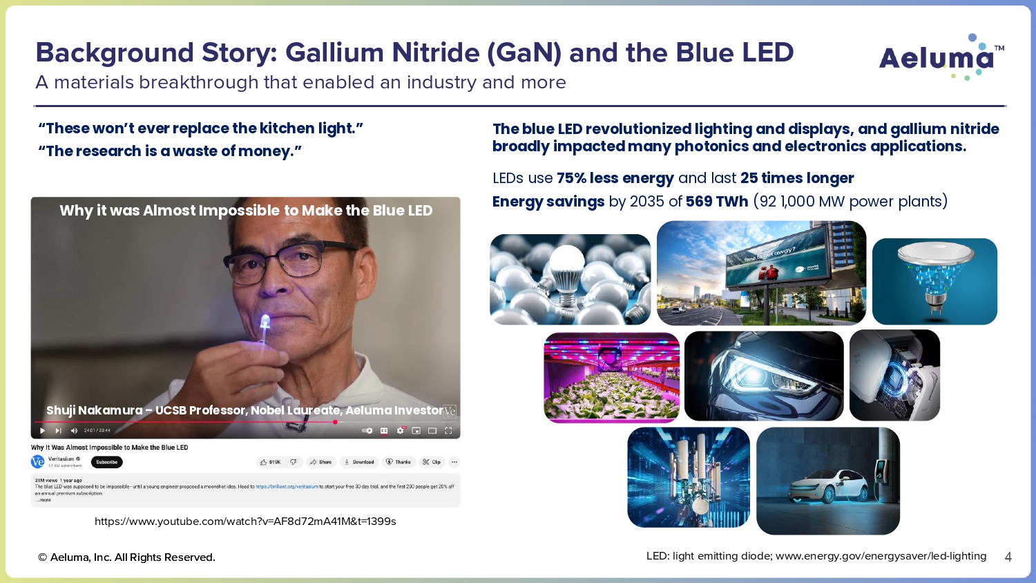
Background Story: Gallium Nitride (GaN) and the Blue LED A materials breakthrough that enabled an industry and more 4 LED: light emitting diode; www.energy.gov/energysaver/led - lighting https:// www.youtube.com/watch?v=AF8d72mA41M&t=1399s The blue LED revolutionized lighting and displays, and gallium nitride broadly impacted many photonics and electronics applications. LEDs use 75% less energy and last 25 times longer Energy savings by 2035 of 569 TWh (92 1,000 MW power plants) “These won’t ever replace the kitchen light.” “The research is a waste of money.” Why it was Almost Impossible to Make the Blue LED Shuji Nakamura – UCSB Professor, Nobel Laureate, Aeluma Investor © Aeluma, Inc. All Rights Reserved.
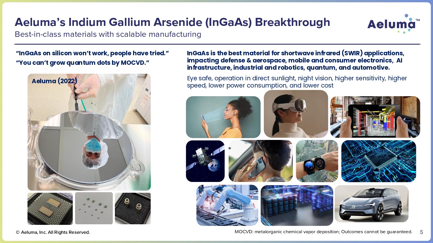
Aeluma’s Indium Gallium Arsenide (InGaAs) Breakthrough Best - in - class materials with scalable manufacturing InGaAs is the best material for shortwave infrared (SWIR) applications, impacting defense & aerospace, mobile and consumer electronics, AI infrastructure, industrial and robotics, quantum, and automotive. Eye safe, operation in direct sunlight, night vision, higher sensitivity, higher speed, lower power consumption, and lower cost “InGaAs on silicon won’t work, people have tried.” “You can’t grow quantum dots by MOCVD.” Aeluma (2022) © Aeluma, Inc. All Rights Reserved. MOCVD: metalorganic chemical vapor deposition; Outcomes cannot be guaranteed. 5
Investment Highlights Derisked business model poised for growth as U.S. recaptures semiconductor preeminence Rapidly Expanding SAM $4.9B in 2030 Broad applications across Defense and Aerospace, Mobile and Consumer Electronics, AI Infrastructure, Quantum, Industrial and Robotics, and Automotive Transformative Technology • Best - in - class materials with large - volume manufacturing • Highest performance at scale • 30+ issued and pending patents Significant Business Traction • Disruptive tech validated by U.S. agencies and customers • Sampling, small volume orders, and NRE contracts • 20 customer engagements Capital - Light Manufacturing • Primarily outsourced manufacturing for rapid scaling • Some proprietary steps carried out in house • ISO9001:2015 certified Clean Balance Sheet • No debt or overhang • $39.2M cash (pro - forma at 6/30) Attractive Financial Profile and Outlook • Recurring R&D revenue • Additional capital to fund business and accelerate commercialization © Aeluma, Inc. All Rights Reserved. SAM estimate based on internal projections; NRE: Non - recurring engineering; Outcomes cannot be guaranteed. 6
Recent Developments FY2025 Results Announced on 9/9/25 Operational and Financial Highlights x Nasdaq IPO (Uplist) and $13.8M capital raise In March x $25.4M capital raise in September x FY2025 revenue $4.7M (up from $0.9M in FY24) x 6 R&D contracts secured in 2025, including 2 in Q4 x 20 active customer engagements x Unveiled scalable manufacturing process applicable to quantum computing and communication systems x Chris Stewart with strong semiconductor and public - company experience appointed CFO x Strong balance sheet with $39.2M in Cash and Cash Equivalents (pro - forma at 6/30) and no debt Strategic Priorities for FY2026 □ New Contract Wins 3 - 7 new R&D contracts □ Team Expansion Accelerate hiring of business development and go - to - market team, technical leadership, and operations □ Enhanced Manufacturing Readiness Higher levels of wafer fab activities, expanded test and validation capabilities, technology qualification for target industries □ Go - to - Market Traction Continued progress with engaged targeted commercial markets and increase customer engagements in pipeline Actively engaged with 20 prospective customers evaluating our technology for potential integration © Aeluma, Inc. All Rights Reserved. Outcomes cannot be guaranteed. 7
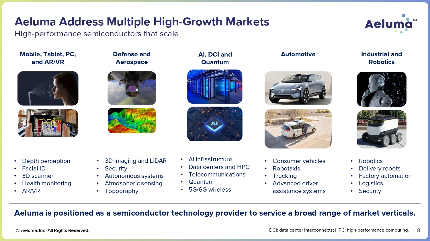
Automotive Aeluma Address Multiple High - Growth Markets High - performance semiconductors that scale 8 • Consumer vehicles • Robotaxis • Trucking • Advanced driver assistance systems Industrial and Robotics Defense and Aerospace Mobile, Tablet, PC, and AR/VR • Robotics • Delivery robots • Factory automation • Logistics • Security • 3D imaging and LiDAR • Security • Autonomous systems • Atmospheric sensing • Topography • Depth perception • Facial ID • 3D scanner • Health monitoring • AR/VR Aeluma is positioned as a semiconductor technology provider to service a broad range of market verticals. AI, DCI and Quantum • AI infrastructure • Data centers and HPC • Telecommunications • Quantum • 5G/6G wireless DCI: data center interconnects; HPC: high - performance computing. © Aeluma, Inc. All Rights Reserved.
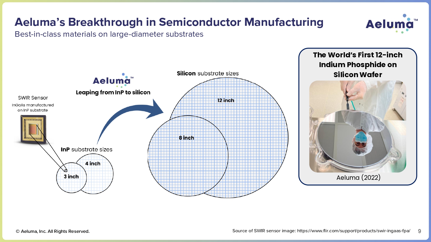
Aeluma’s Breakthrough in Semiconductor Manufacturing Best - in - class materials on large - diameter substrates 9 Source of SWIR sensor image: https:// www.flir.com/support/products/swir - ingaas - fpa/ The World’s First 12 - inch Indium Phosphide on Silicon Wafer Aeluma (2022) © Aeluma, Inc. All Rights Reserved.
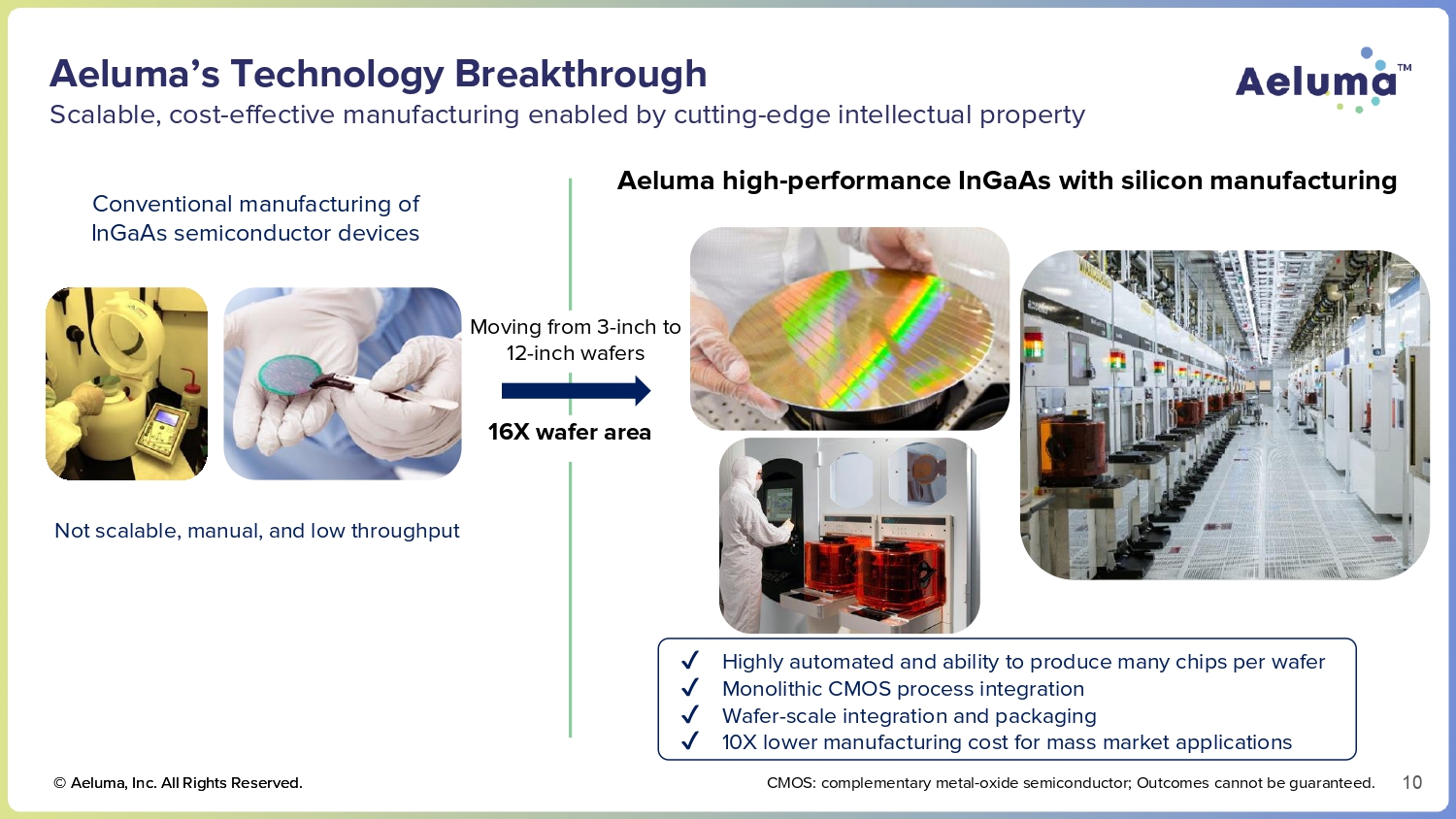
Not scalable, manual, and low throughput Highly automated and ability to produce many chips per wafer Monolithic CMOS process integration Wafer - scale integration and packaging 10X lower manufacturing cost for mass market applications CMOS: complementary metal - oxide semiconductor; Outcomes cannot be guaranteed. Aeluma’s Technology Breakthrough Scalable, cost - effective manufacturing enabled by cutting - edge intellectual property Aeluma high - performance InGaAs with silicon manufacturing Conventional manufacturing of InGaAs semiconductor devices Moving from 3 - inch to 12 - inch wafers 16X wafer area 10 © Aeluma, Inc. All Rights Reserved.
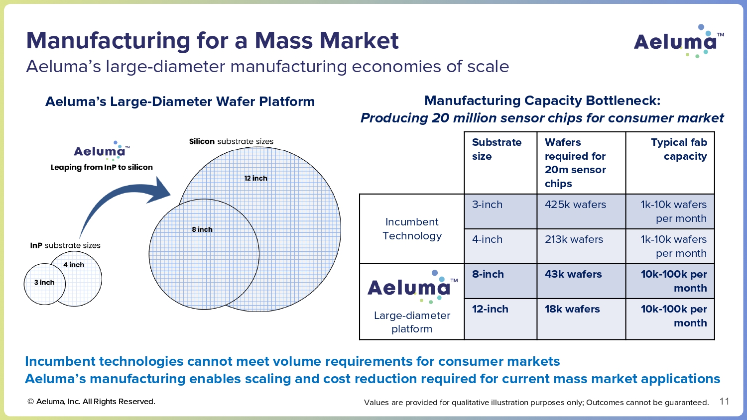
Manufacturing for a Mass Market Aeluma’s large - diameter manufacturing economies of scale Incumbent technologies cannot meet volume requirements for consumer markets Aeluma’s manufacturing enables scaling and cost reduction required for current mass market applications Typical fab capacity Wafers required for 20m sensor chips Substrate size 1k - 10k wafers per month 425k wafers 3 - inch Incumbent Technology 1k - 10k wafers per month 213k wafers 4 - inch 10k - 100k per month 43k wafers 8 - inch Large - diameter platform 10k - 100k per month 18k wafers 12 - inch Manufacturing Capacity Bottleneck: Producing 20 million sensor chips for consumer market Aeluma’s Large - Diameter Wafer Platform © Aeluma, Inc. All Rights Reserved. Values are provided for qualitative illustration purposes only; Outcomes cannot be guaranteed. 11
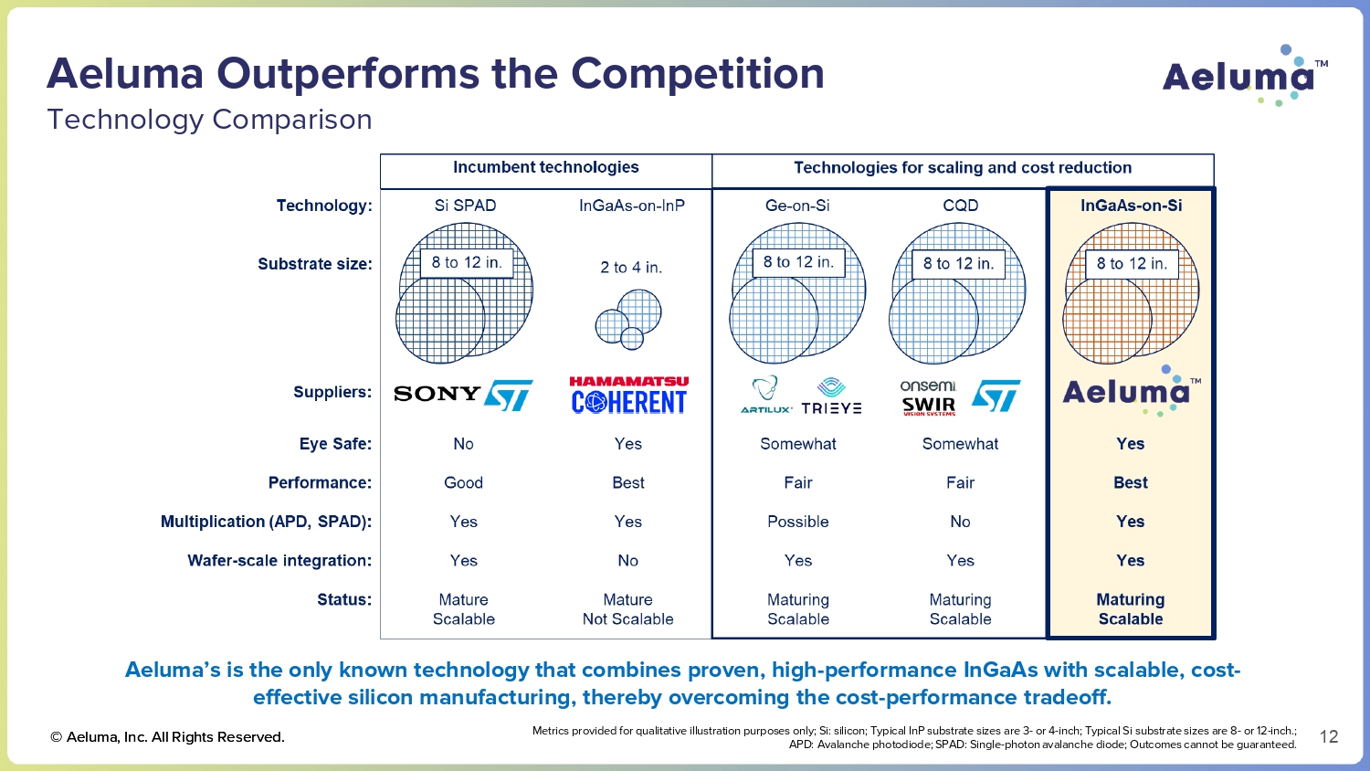
APD: Avalanche photodiode; SPAD: Single - photon avalanche diode; Outcomes cannot be guaranteed. Aeluma Outperforms the Competition Technology Comparison Aeluma’s is the only known technology that combines proven, high - performance InGaAs with scalable, cost - effective silicon manufacturing, thereby overcoming the cost - performance tradeoff. Metrics provided for qualitative illustration purposes only; Si: silicon; Typical InP substrate sizes are 3 - or 4 - inch; Typical Si substrate sizes are 8 - or 12 - inch.; 12 © Aeluma, Inc. All Rights Reserved.
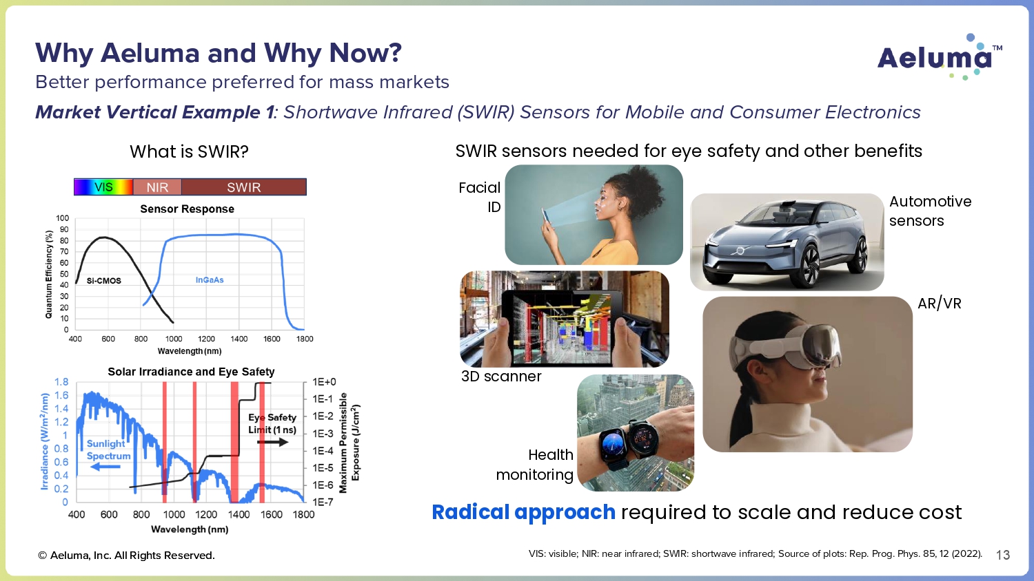
Why Aeluma and Why Now? 13 Better performance preferred for mass markets Market Vertical Example 1 : Shortwave Infrared (SWIR) Sensors for Mobile and Consumer Electronics What is SWIR? SWIR sensors needed for eye safety and other benefits Facial ID 3D scanner Health monitoring Radical approach required to scale and reduce cost VIS: visible; NIR: near infrared; SWIR: shortwave infrared; Source of plots: Rep. Prog. Phys. 85, 12 (2022). AR/VR Automotive sensors © Aeluma, Inc. All Rights Reserved.
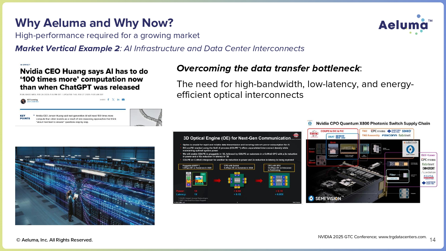
Why Aeluma and Why Now? High - performance required for a growing market Market Vertical Example 2 : AI Infrastructure and Data Center Interconnects Overcoming the data transfer bottleneck : The need for high - bandwidth, low - latency, and energy - efficient optical interconnects NVIDIA 2025 GTC Conference; www.trgdatacenters.com. © Aeluma, Inc. All Rights Reserved. 14
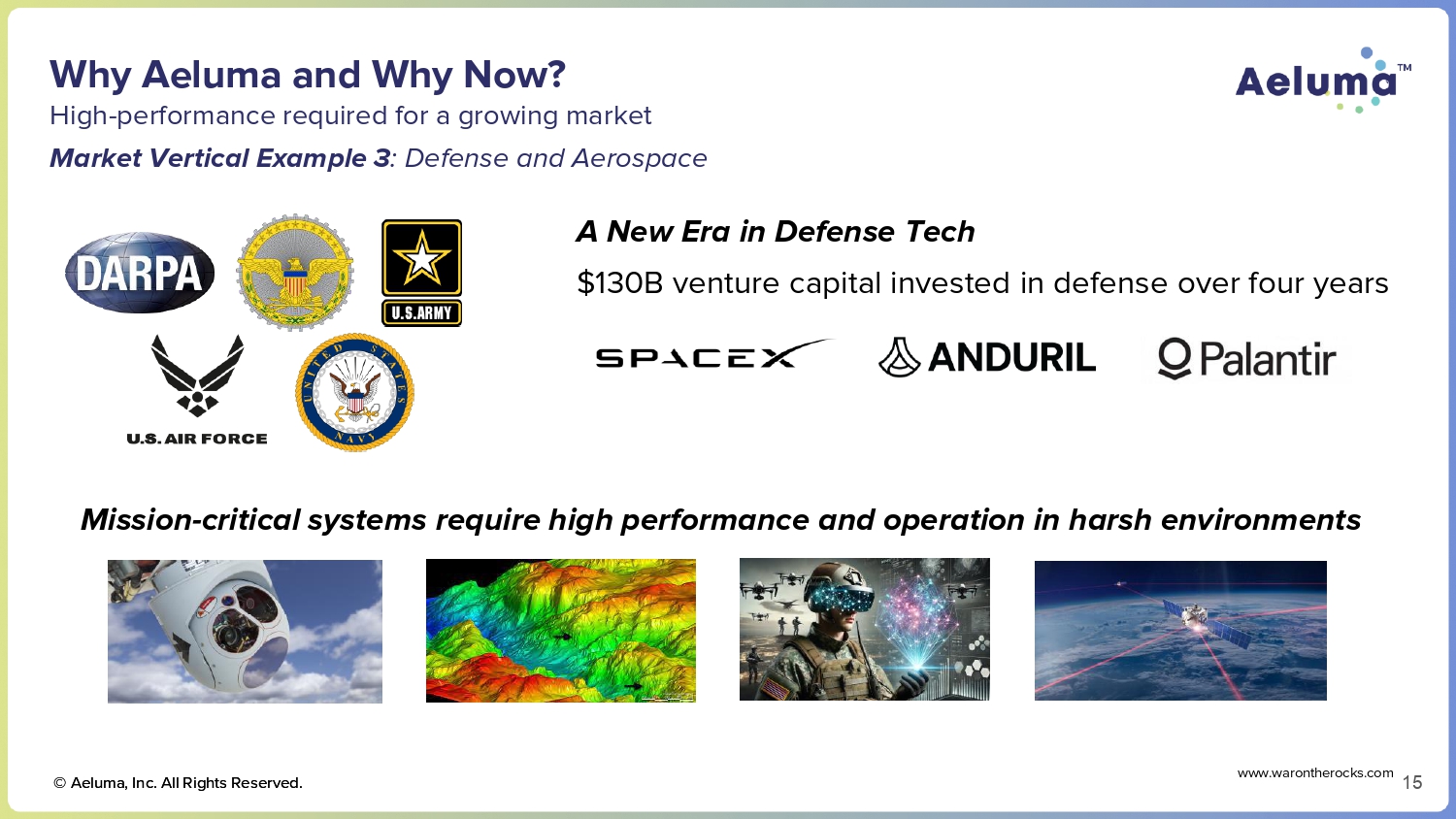
Why Aeluma and Why Now? High - performance required for a growing market Market Vertical Example 3 : Defense and Aerospace A New Era in Defense Tech $130B venture capital invested in defense over four years Mission - critical systems require high performance and operation in harsh environments www.warontherocks.com © Aeluma, Inc. All Rights Reserved. 15
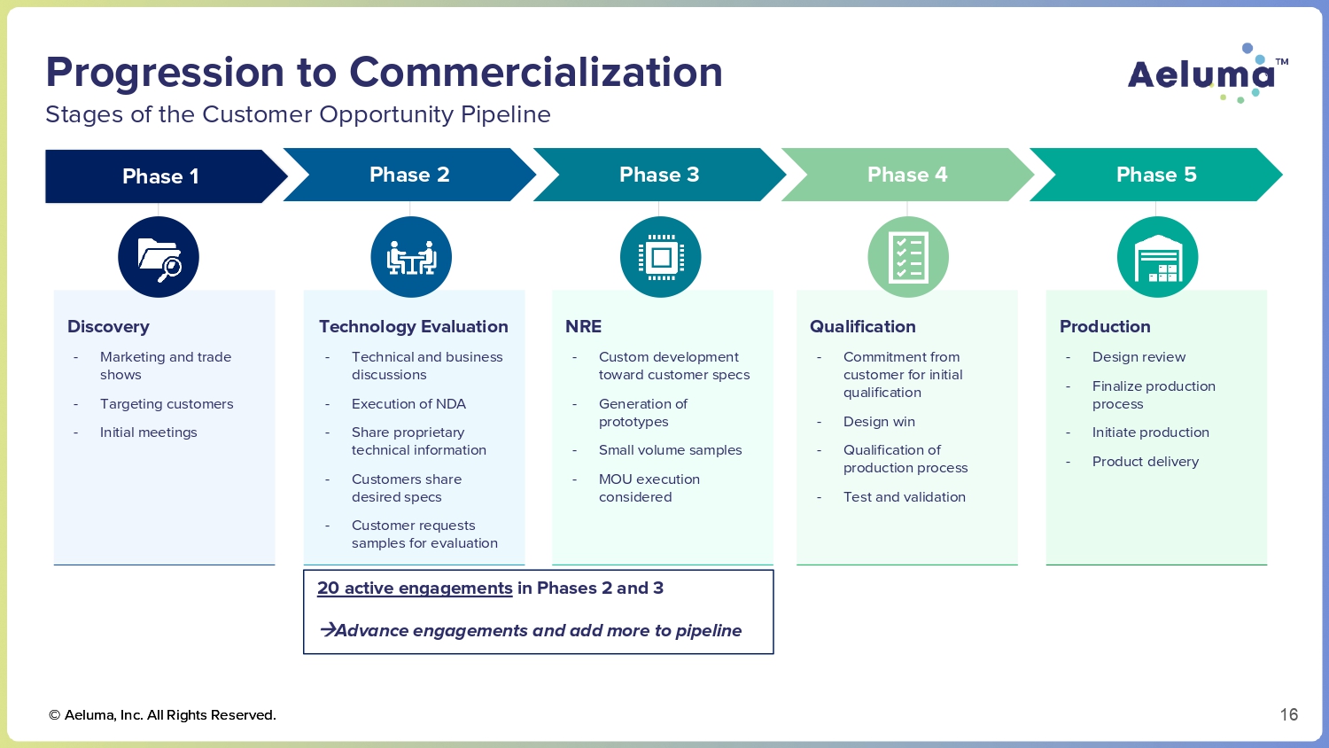
Discovery - Marketing and trade shows - Targeting customers - Initial meetings Qualification - Commitment from customer for initial qualification - Design win - Qualification of production process - Test and validation Phase 1 Phase 2 Phase 3 Phase 4 Phase 5 Production © Aeluma, Inc. All Rights Reserved. 16 - Design review - Finalize production process - Initiate production - Product delivery NRE - Custom development toward customer specs - Generation of prototypes - Small volume samples - MOU execution considered Technology Evaluation - Technical and business discussions - Execution of NDA - Share proprietary technical information - Customers share desired specs - Customer requests samples for evaluation 20 active engagements in Phases 2 and 3 Advance engagements and add more to pipeline Progression to Commercialization Stages of the Customer Opportunity Pipeline
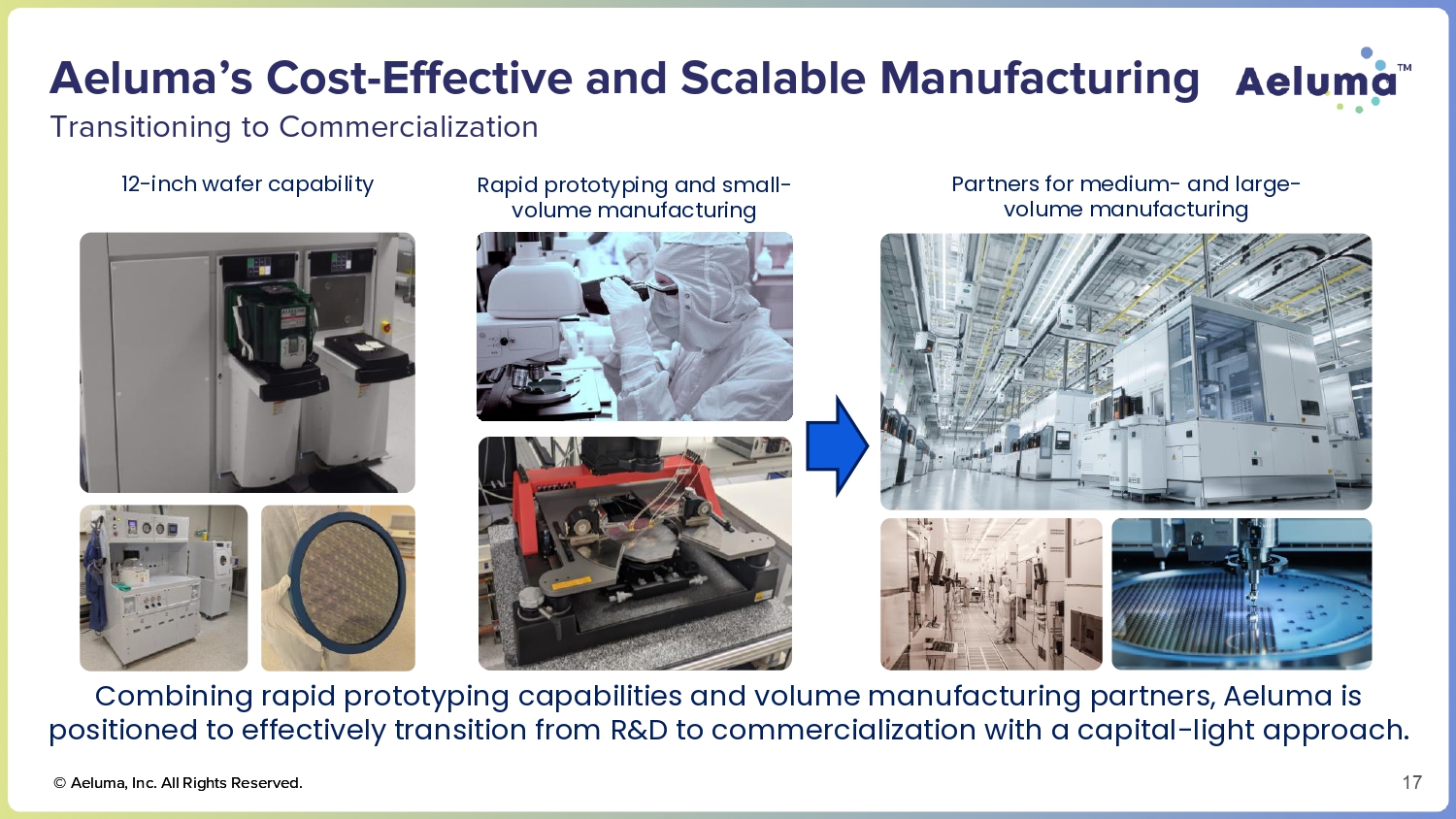
Aeluma’s Cost - Effective and Scalable Manufacturing Transitioning to Commercialization 12 - inch wafer capability Combining rapid prototyping capabilities and volume manufacturing partners, Aeluma is positioned to effectively transition from R&D to commercialization with a capital - light approach. Rapid prototyping and small - volume manufacturing Partners for medium - and large - volume manufacturing © Aeluma, Inc. All Rights Reserved. 17
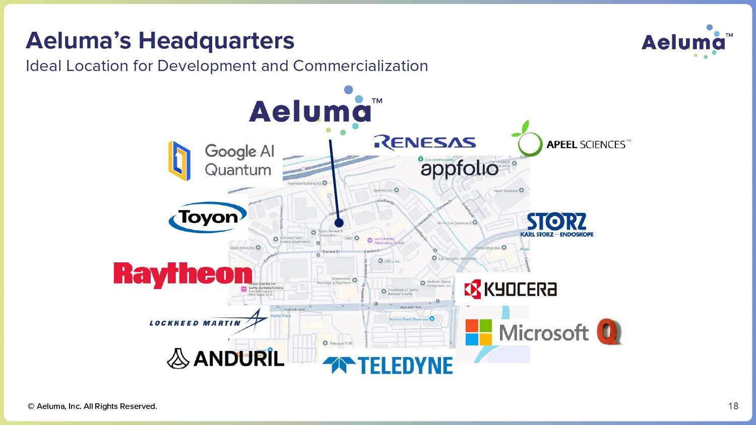
Aeluma’s Headquarters Ideal Location for Development and Commercialization © Aeluma, Inc. All Rights Reserved. 18
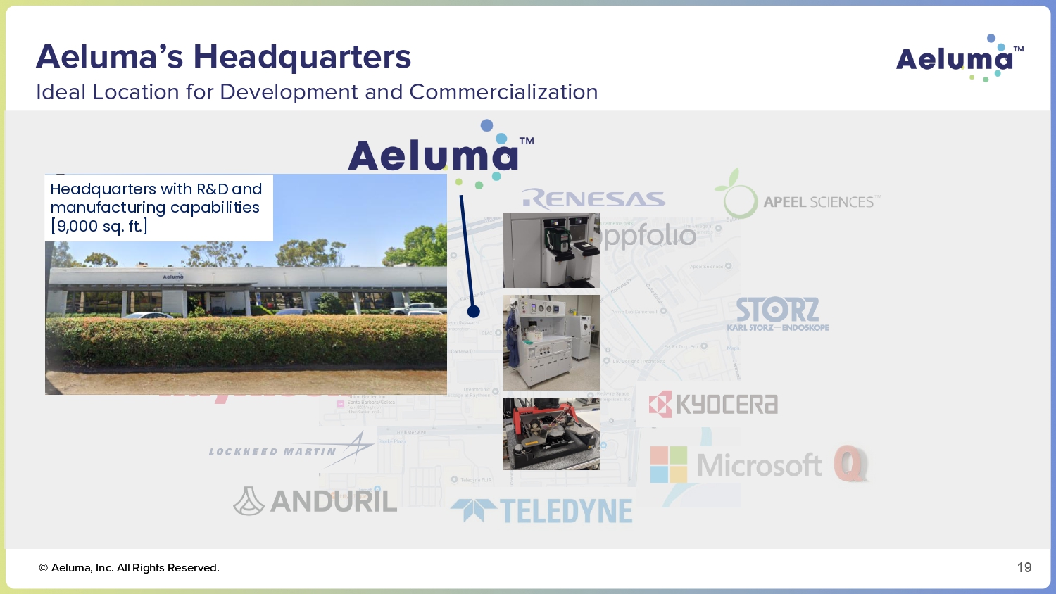
Aeluma’s Headquarters Ideal Location for Development and Commercialization Headquarters with R&D and manufacturing capabilities [ 9 , 000 sq . ft . ] © Aeluma, Inc. All Rights Reserved. 19
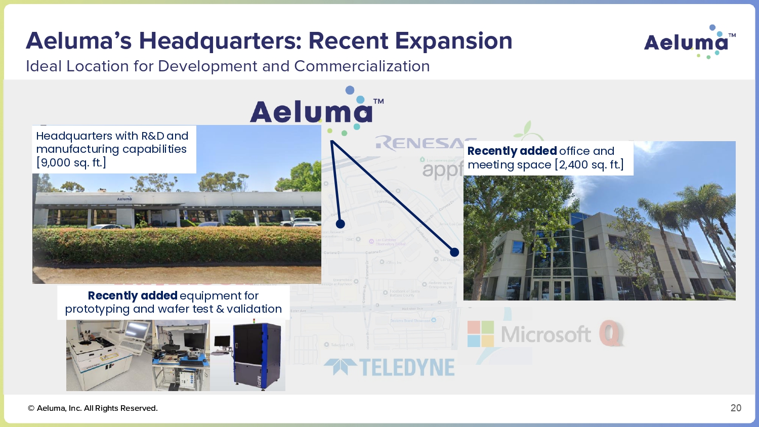
Aeluma’s Headquarters: Recent Expansion Ideal Location for Development and Commercialization Headquarters with R&D and manufacturing capabilities [ 9 , 000 sq . ft . ] Recently added equipment for prototyping and wafer test & validation Recently added office and meeting space [2,400 sq. ft.] © Aeluma, Inc. All Rights Reserved. 20
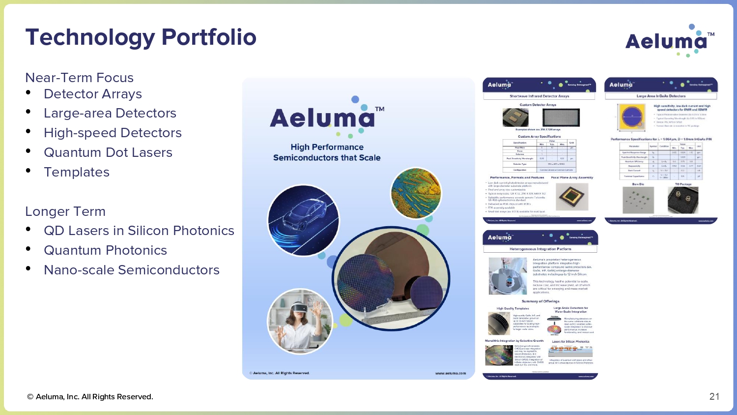
Technology Portfolio © Aeluma, Inc. All Rights Reserved. 21 Near - Term Focus • Detector Arrays • Large - area Detectors • High - speed Detectors • Quantum Dot Lasers • Templates Longer Term • QD Lasers in Silicon Photonics • Quantum Photonics • Nano - scale Semiconductors
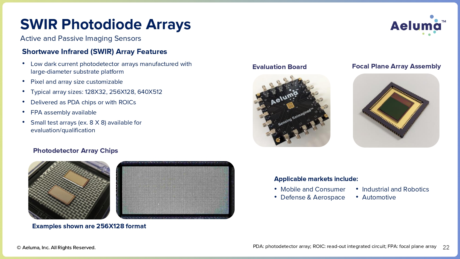
SWIR Photodiode Arrays Active and Passive Imaging Sensors Shortwave Infrared (SWIR) Array Features • Low dark current photodetector arrays manufactured with large - diameter substrate platform • Pixel and array size customizable • Typical array sizes: 128X32, 256X128, 640X512 • Delivered as PDA chips or with ROICs • FPA assembly available • Small test arrays (ex. 8 X 8) available for evaluation/qualification Examples shown are 256X128 format Focal Plane Array Assembly Evaluation Board PDA: photodetector array; ROIC: read - out integrated circuit; FPA: focal plane array © Aeluma, Inc. All Rights Reserved. 22 Photodetector Array Chips • Mobile and Consumer • Defense & Aerospace • Industrial and Robotics • Automotive Applicable markets include:
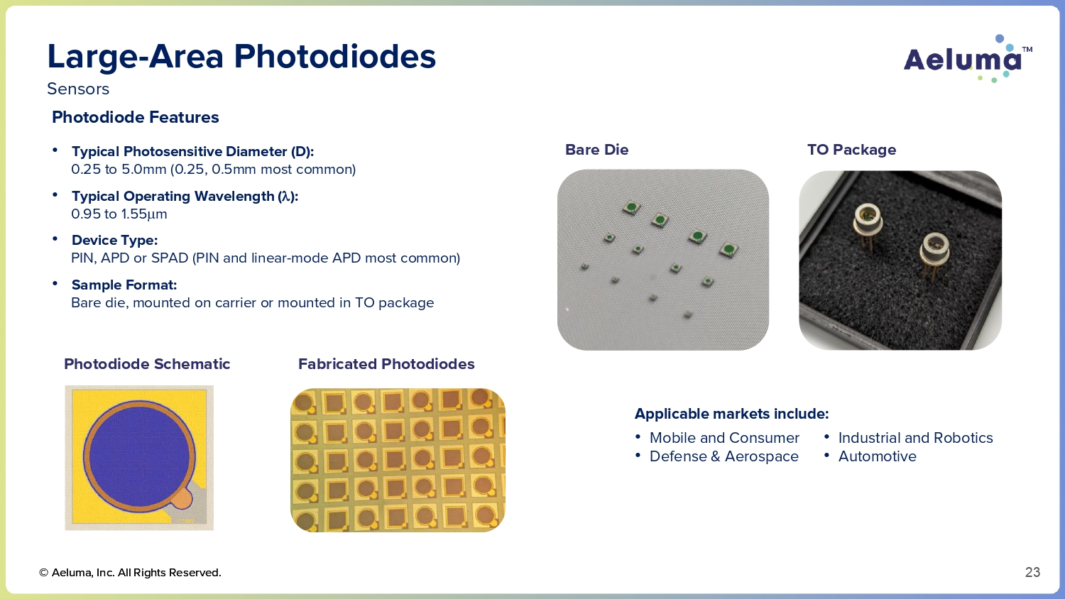
Large - Area Photodiodes Sensors Photodiode Features • Typical Photosensitive Diameter (D): 0.25 to 5.0mm (0.25, 0.5mm most common) • Typical Operating Wavelength ( ): 0.95 to 1.55 m • Device Type: PIN, APD or SPAD (PIN and linear - mode APD most common) • Sample Format: Bare die, mounted on carrier or mounted in TO package Bare Die TO Package Photodiode Schematic Fabricated Photodiodes © Aeluma, Inc. All Rights Reserved. 23 • Mobile and Consumer • Defense & Aerospace • Industrial and Robotics • Automotive Applicable markets include:
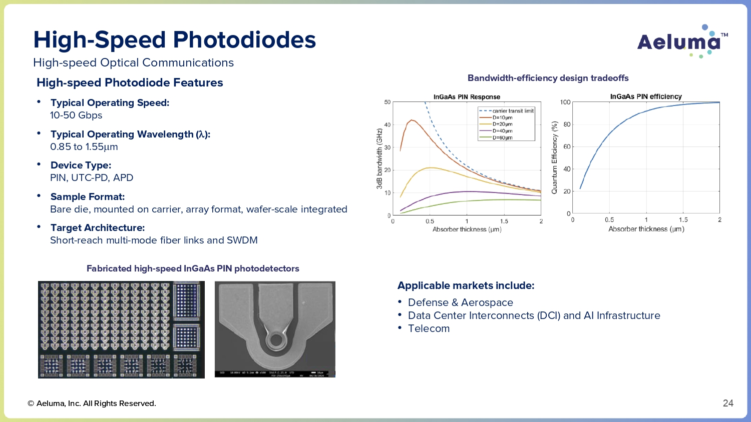
High - Speed Photodiodes Bandwidth - efficiency design tradeoffs High - speed Optical Communications High - speed Photodiode Features © Aeluma, Inc. All Rights Reserved. 24 • Typical Operating Speed: 10 - 50 Gbps • Typical Operating Wavelength ( ): 0.85 to 1.55 m • Device Type: PIN, UTC - PD, APD • Sample Format: Bare die, mounted on carrier, array format, wafer - scale integrated • Target Architecture: Short - reach multi - mode fiber links and SWDM Fabricated high - speed InGaAs PIN photodetectors Applicable markets include: • Defense & Aerospace • Data Center Interconnects (DCI) and AI Infrastructure • Telecom
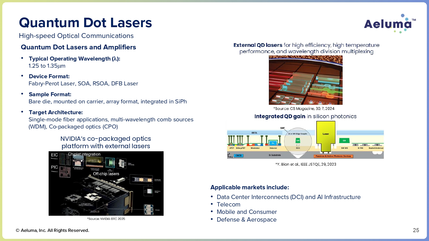
Quantum Dot Lasers Applicable markets include: • Data Center Interconnects (DCI) and AI Infrastructure • Telecom • Mobile and Consumer • Defense & Aerospace High - speed Optical Communications Quantum Dot Lasers and Amplifiers • Typical Operating Wavelength ( ): 1.25 to 1.35 m • Device Format: Fabry - Perot Laser, SOA, RSOA, DFB Laser • Sample Format: Bare die, mounted on carrier, array format, integrated in SiPh • Target Architecture: Single - mode fiber applications, multi - wavelength comb sources (WDM), Co - packaged optics (CPO) NVIDIA’s co - packaged optics platform with external lasers © Aeluma, Inc. All Rights Reserved. 25
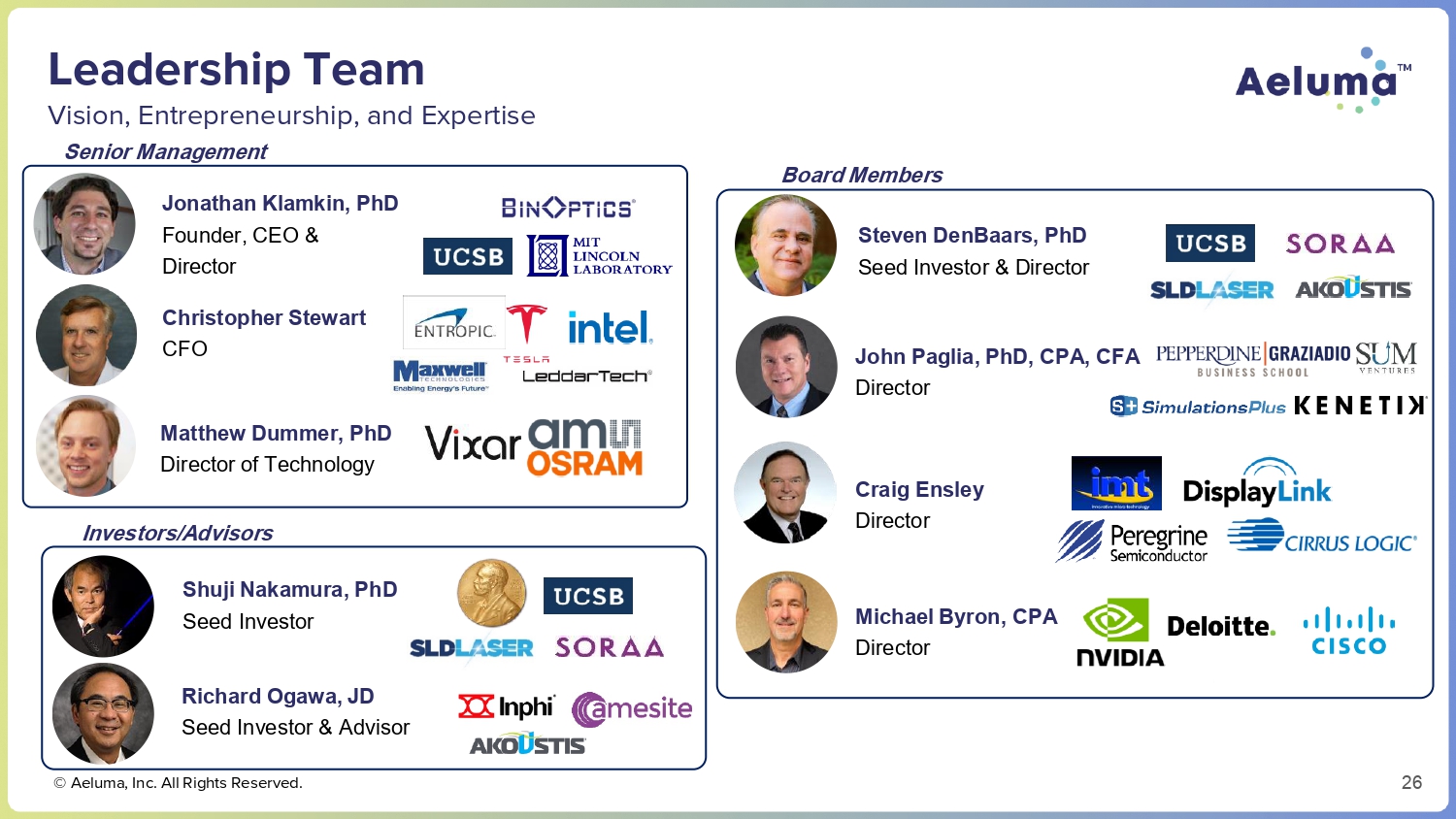
Leadership Team Steven DenBaars, PhD Seed Investor & Director John Paglia, PhD, CPA, CFA Director Craig Ensley Director Shuji Nakamura, PhD Seed Investor Richard Ogawa, JD Seed Investor & Advisor Vision, Entrepreneurship, and Expertise Senior Management Board Members Investors/Advisors Michael Byron, CPA Director Jonathan Klamkin, PhD Founder, CEO & Director Christopher Stewart CFO Matthew Dummer, PhD Director of Technology © Aeluma, Inc. All Rights Reserved. 26
© Aeluma, Inc. All Rights Reserved. info@aeluma.com | www.aeluma.com © Aeluma, Inc. All Rights Reserved.