Exhibit 99.4
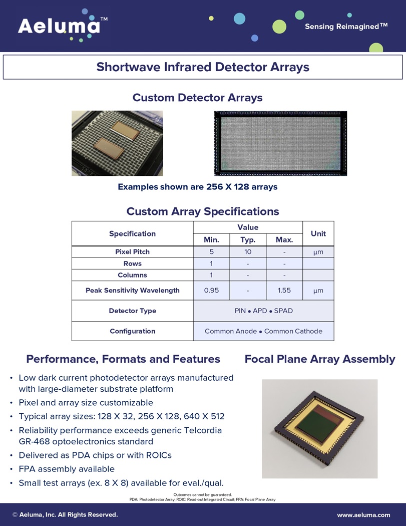
Sensing Reimagined TM Shortwave Infrared Detector Arrays Performance, Formats and Features • Low dark current photodetector arrays manufactured with large - diameter substrate platform • Pixel and array size customizable • Typical array sizes: 128 X 32, 256 X 128, 640 X 512 • Reliability performance exceeds generic Telcordia GR - 468 optoelectronics standard • Delivered as PDA chips or with ROICs • FPA assembly available • Small test arrays (ex. 8 X 8) available for eval./qual. Examples shown are 256 X 128 arrays Custom Array Specifications Unit Value Specification Max. Typ. Min. μ m - 10 5 Pixel Pitch - - 1 Rows - - 1 Columns μ m 1.55 - 0.95 Peak Sensitivity Wavelength PIN APD SPAD Detector Type Common Anode Common Cathode Configuration Focal Plane Array Assembly Custom Detector Arrays © Aeluma, Inc. All Rights Reserved. www.aeluma.com Outcomes cannot be guaranteed. PDA: Photodetector Array; ROIC: Read - out Integrated Circuit; FPA: Focal Plane Array
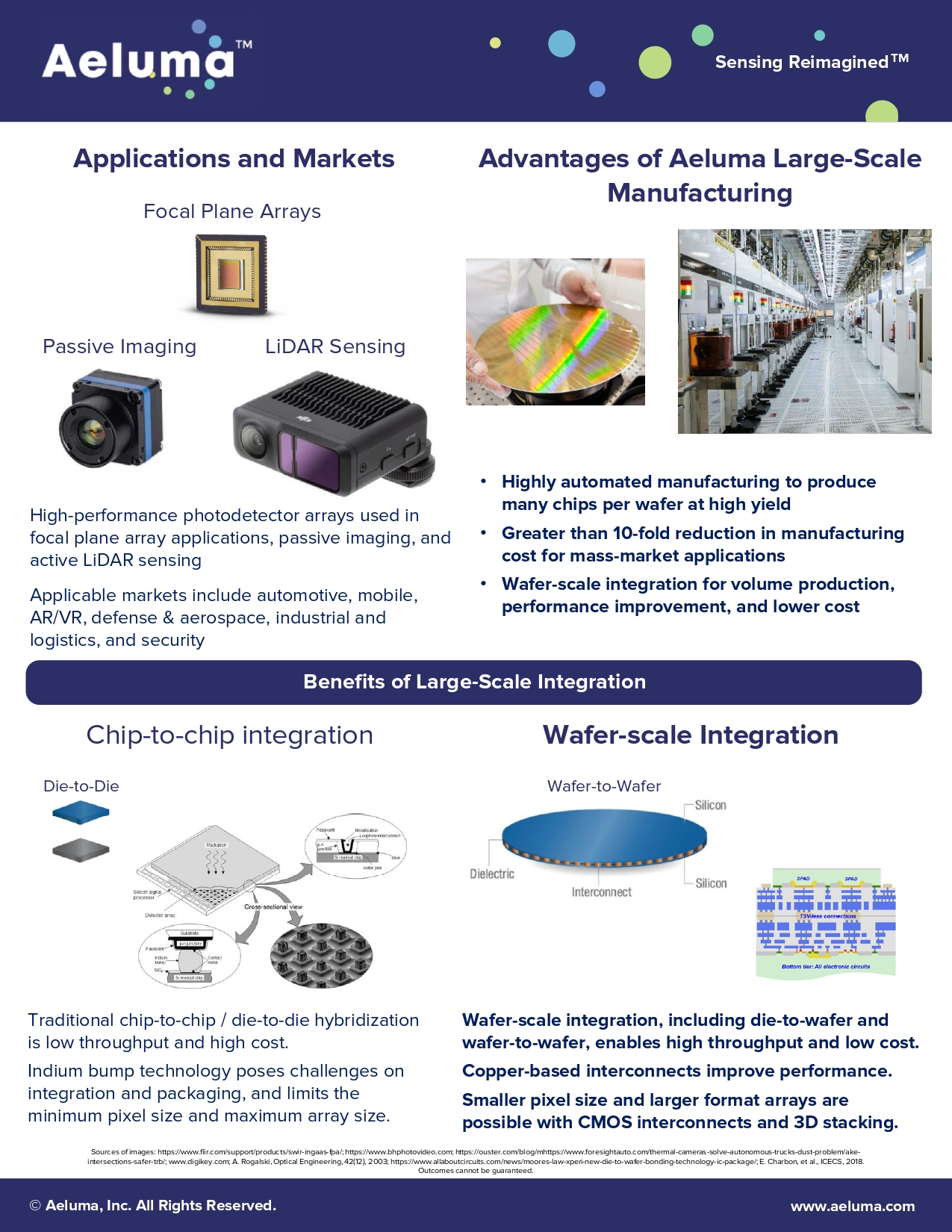
Sensing Reimagined TM Applications and Markets Focal Plane Arrays Sources of images: https://www.flir.com/support/products/swir - ingaas - fpa/; https://www.bhphotovideo.com; https://ouster.com/blog/mhttps:// www.foresightauto.com/thermal - cameras - solve - autonomous - trucks - dust - problem/ake - intersections - safer - trb/; www.digikey.com; A. Rogalski, Optical Engineering, 42(12), 2003; https:// www.allaboutcircuits.com/news/moores - law - xperi - new - die - to - wafer - bonding - technology - ic - package/; E. Charbon, et al., ICECS, 2018. Outcomes cannot be guaranteed. Advantages of Aeluma Large - Scale Manufacturing Passive Imaging LiDAR Sensing Benefits of Large - Scale Integration • Highly automated manufacturing to produce many chips per wafer at high yield • Greater than 10 - fold reduction in manufacturing cost for mass - market applications • Wafer - scale integration for volume production, performance improvement, and lower cost © Aeluma, Inc. All Rights Reserved. www.aeluma.com High - performance photodetector arrays used in focal plane array applications, passive imaging, and active LiDAR sensing Applicable markets include automotive, mobile, AR/VR, defense & aerospace, industrial and logistics, and security Chip - to - chip integration Die - to - Die Wafer - scale Integration Wafer - to - Wafer Traditional chip - to - chip / die - to - die hybridization is low throughput and high cost. Indium bump technology poses challenges on integration and packaging, and limits the minimum pixel size and maximum array size. Wafer - scale integration, including die - to - wafer and wafer - to - wafer, enables high throughput and low cost. Copper - based interconnects improve performance. Smaller pixel size and larger format arrays are possible with CMOS interconnects and 3D stacking.