Exhibit 99.1
Sen s i ng Rei ma g i n e d TM L a rge - W a fer Het erog e neously In t egr a t e d InG a As Pho t ode t ec tor Sensors Matthew Dummer , Jonathan Klamkin, Bei Shi, Bowen Song, Simone S. Brunelli, Michael McGivney, Douglas Oakley, Daniel Renner P a per 1 2 88 0 - 18 J an u a r y 30, 2 0 24 © Aelu m a , Inc. All R i g ht s R e serve d .
Outline © Aelu m a , Inc. All R i g ht s R e serve d . ● I ntrodu c tion to Aeluma ● Background on InGaAs detectors and scaling limitations ● Aeluma’s scalable large - diameter wafer platform ● D e te ct o r array p e rf o rma nce re s ults ● C o mparison to o ther de te ct o r te c h nologi e s ● Summary of product and technology offerings ● Conclusions
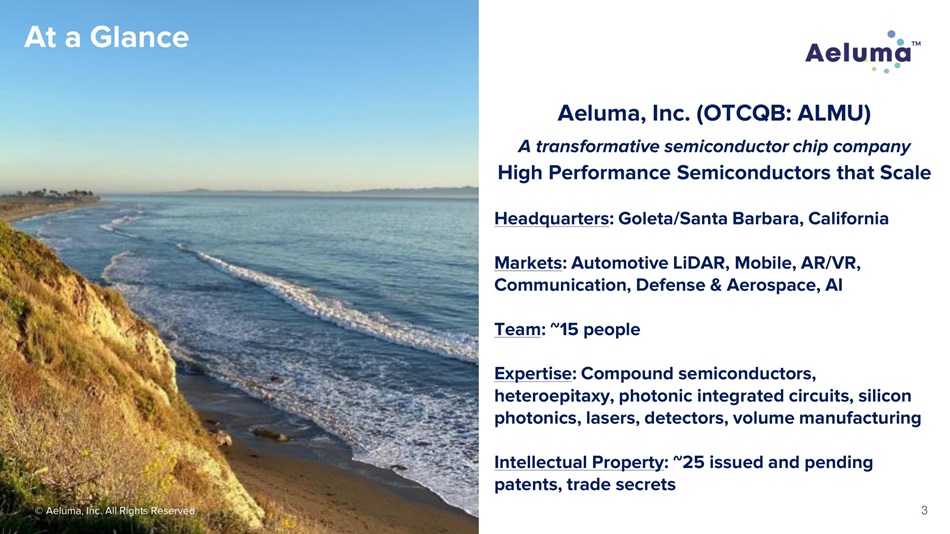
© Aelu m a , Inc. All R i g ht s R e serve d . At a Glance Aeluma, Inc. (O T C Q B : AL M U) A transformative semiconductor chip company High P e rf o rma nce S e mic o nduct o rs that Scale Headquarters : Goleta/Santa Barbara, California Ma rk e t s : Au t omot i v e LiDAR, Mob i l e, AR/VR, Communication, Defense & Aerospace, AI Te a m : ~15 people Ex p er t i s e : C ompound se mi c on d uct o r s , he t eroep i t a x y , photon i c i n t e gra t e d circ u i t s , s i l i c on photon i c s, l ase rs, d e t ectors, volume ma nu fact u r i ng I n t e l l ect ua l Pro p e r t y : ~25 i ss u e d a nd pen d i ng pat en t s, t rad e secr e t s 3
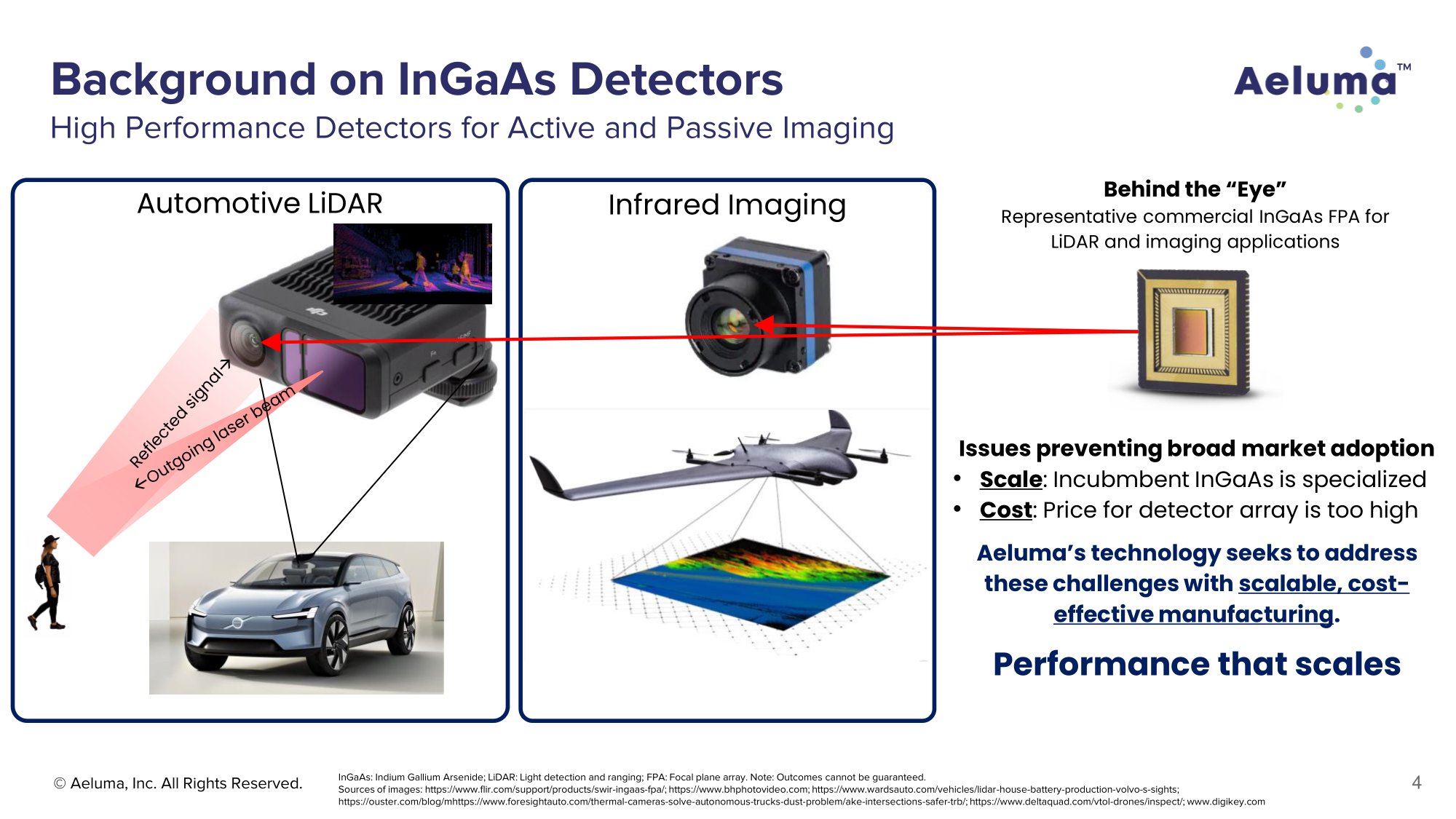
Background on InGaAs Detectors High Performance Detectors for Active and Passive Imaging © Aelu m a , Inc. All R i g ht s R e serve d . 4 InGaAs: Indium Gallium Arsenide; LiDAR: Light detection and ranging; FPA: Focal plane array. Note: Outcomes cannot be guaranteed. Sources of images: https://www.flir.com/support/products/swir - ingaas - fpa/; https://www.bhphotovideo.com; https:// www.wardsauto.com/vehicles/lidar - house - battery - production - volvo - s - sights; https://ouster.com/blog/mhttps://www.foresightauto.com/thermal - cameras - solve - autonomous - trucks - dust - problem/ake - intersections - sa fer - trb/; https:// www.deltaquad.com/vtol - drones/inspect/; www.digikey.com Be h i n d t h e “ E y e” Representative commercial InGaAs FPA for L i DA R a nd i m a g i ng a pp li c a t i ons I s s ue s p r e v e n t ing b r o a d m a r ke t a d o p t ion • S c a le : I ncub m b e n t I nGaAs i s speciali zed • Cost : Price for detector array is too high A elu m a ’s t e c hno l o g y se e k s t o a dd r e s s t he s e c h a l l e n g e s w i t h s c a l a b le , c o s t - e ffec t iv e m a nuf a c t u r in g . Perform a nce th at s c ales Automotive LiDAR Infrared Imaging
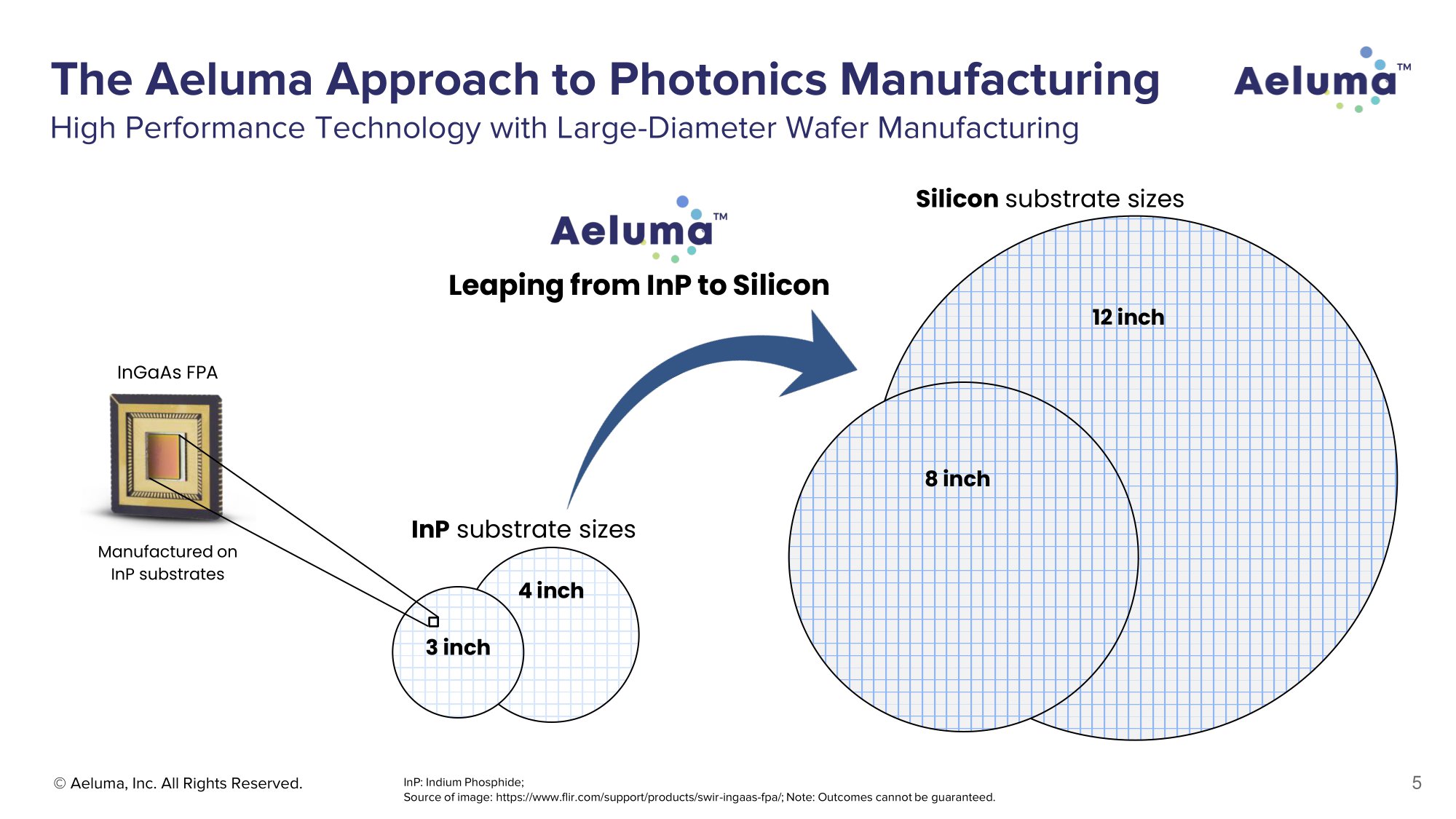
The Aeluma Approach to Photonics Manufacturing High Performance Technology with Large - Diameter Wafer Manufacturing © Aelu m a , Inc. All R i g ht s R e serve d . 5 In P : In d i u m P h o s p h i d e ; Source of image: https:// www.flir.com/support/products/swir - ingaas - fpa/; Note: Outcomes cannot be guaranteed. I n P subs t ra t e si z es I nG a A s F P A M a nu f a c t ur e d on InP substrates 4 in c h 3 in c h 8 in c h Silicon substrate sizes Lea p i ng from I nP t o S ili c o n 12 i n ch
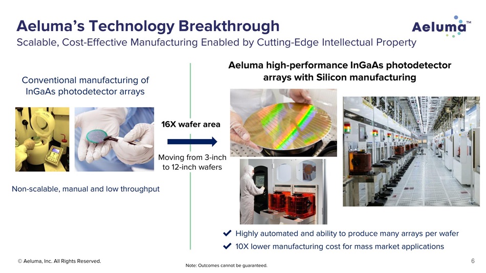
Conventional manufacturing of I n G aA s ph oto d etect or a r r ays arrays with Si l i c on m an u fac t u ri n g Highly automated and ability to produce many arrays per wafer 10X lower manufacturing cost for mass market applications 1 6 X w a fer a re a Movi ng f r om 3 - i nch t o 12 - i nc h w af e rs Non - scalable, manual and low throughput Note: Outcomes cannot be guaranteed. © Aelu m a , Inc. All R i g ht s R e serve d . Aeluma’s Technology Breakthrough Scalable, Cost - Effective Manufacturing Enabled by Cutting - Edge Intellectual Property Aeluma high - performance InGaAs photodetector 6
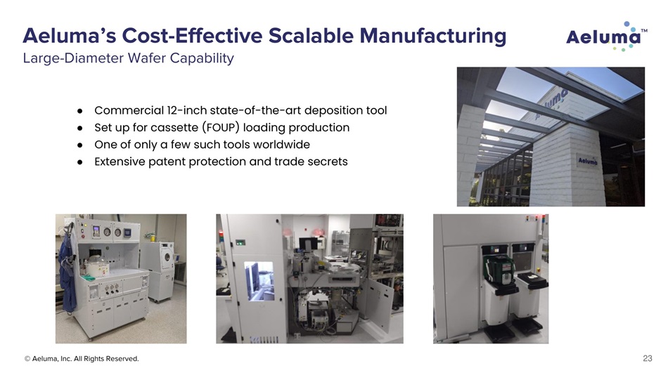
Aeluma’s Cost - Effective Scalable Manufacturing Large - Diameter Wafer Capability ● Commercial 12 - inch state - of - the - art deposition tool ● Set up for cassette (FOUP) loading production ● One of only a few such tools worldwide ● Extensive patent protection and trade secrets © Aelu m a , Inc. All R i g ht s R e serve d . 23
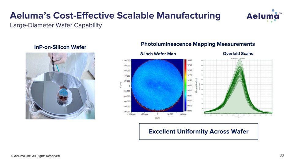
Aeluma’s Cost - Effective Scalable Manufacturing Large - Diameter Wafer Capability Phot olum i n e s ce n c e Ma p p i ng Me a su re m e n t s 8 - i n ch Wafer M ap O ver l aid Scan s Excellent Uniformity Across Wafer InP - o n - Si l i c on W a fer © Aelu m a , Inc. All R i g ht s R e serve d . 23
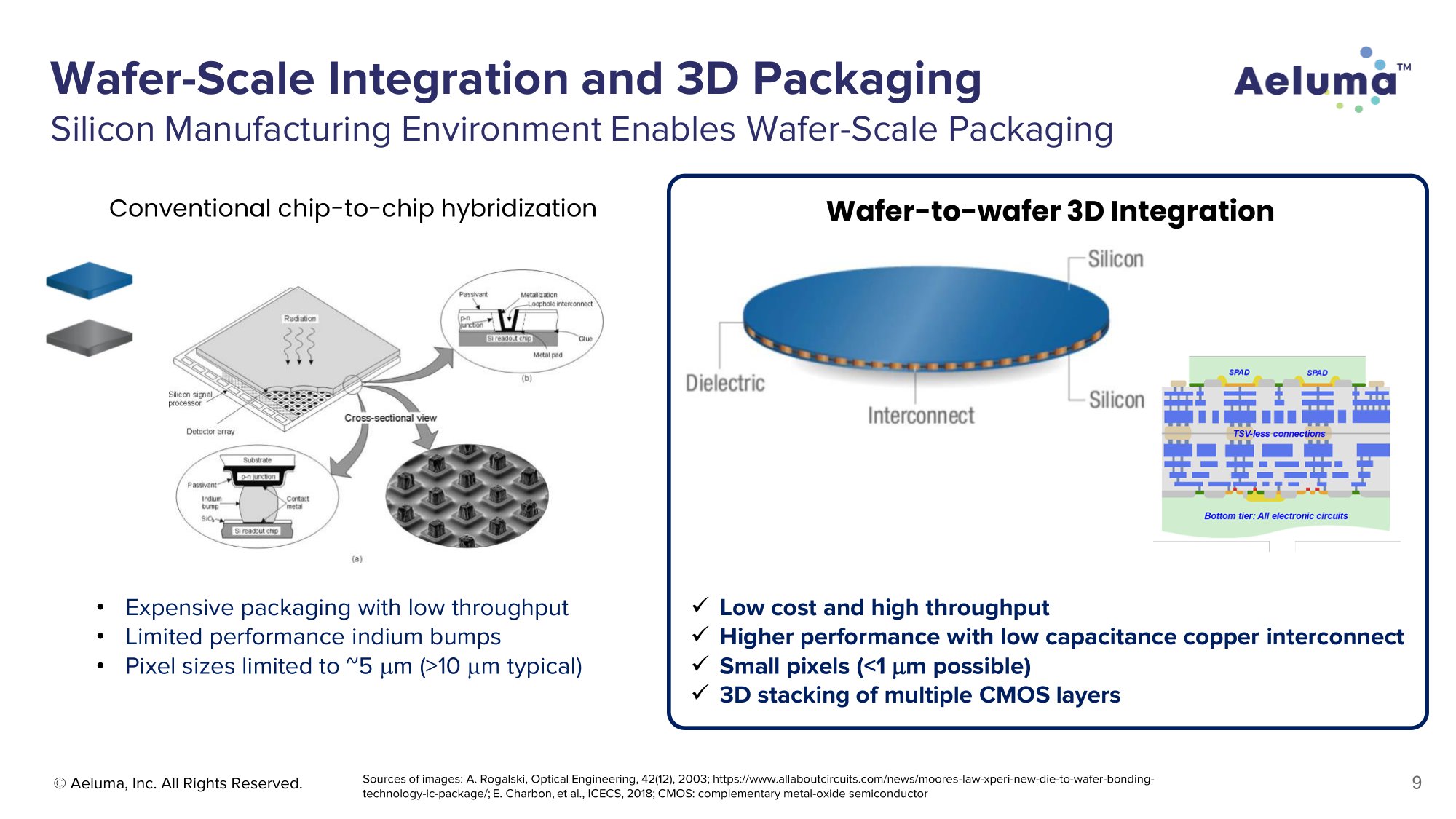
Wafer - Scale Integration and 3D Packaging Silicon Manufacturing Environment Enables Wafer - Scale Packaging © Aelu m a , Inc. All R i g ht s R e serve d . 9 Sources of images: A. Rogalski, Optical Engineering, 42(12), 2003; https:// www.allaboutcircuits.com/news/moores - law - xperi - new - die - to - wafer - bonding - Conventional chip - to - chip hybridization W a fe r - to - w a fer 3 D I n t egra t i on • Ex p e ns i ve pa c kagi ng w i t h l ow t hr o u g h p ut • Limited performance indium bumps • P i x e l s i z e s l im i t e d to ~5 m (> 10 m t ypic a l ) x Low cost and high throughput x Higher performance with low capacitance copper interconnect x Sm a ll p i x e l s ( < 1 m p o s s ibl e ) x 3D stacking of multiple CMOS layers technology - ic - package/; E. Charbon, et al., ICECS, 2018; CMOS: complementary metal - oxide semiconductor
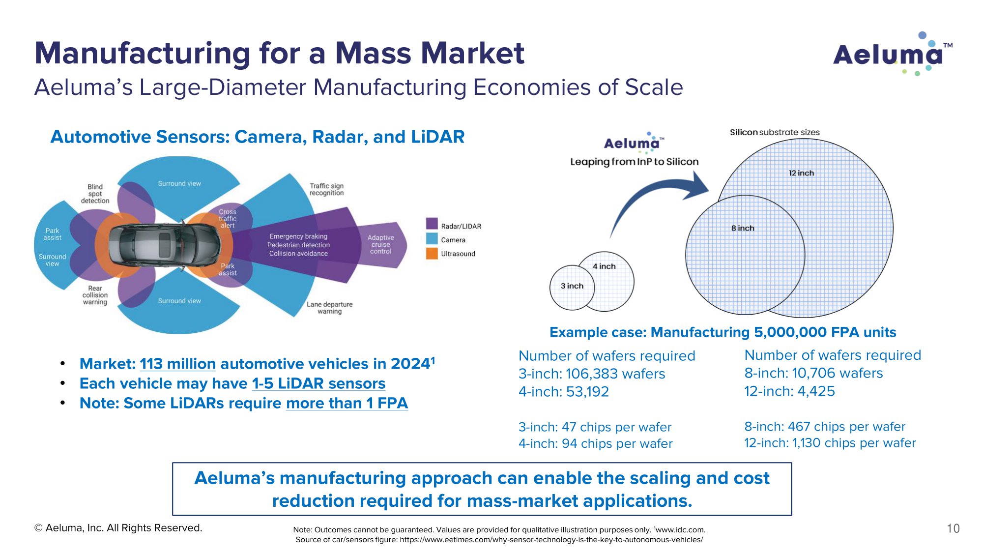
Manufactu ring for a Mass Market Aeluma’s Large - Diameter Manufacturing Economies of Scale Automotive Sensors: Camera, Radar, and LiDAR © Aelu m a , Inc. All R i g ht s R e serve d . 10 Note: Outcomes cannot be guaranteed. Values are provided for qualitative illustration purposes only. 1 www.idc.com. • M ar k et: 11 3 m i l l i o n aut o m o ti v e v eh icl e s in 202 4 1 • E ach v eh i cle m a y ha v e 1 - 5 L iDA R sens o rs • N o te: So m e L iDA Rs r e q uire m o r e tha n 1 FPA Number o f wa fers r e q u ir ed 3 - i n c h: 1 0 6 , 3 8 3 wa fers 4 - i n c h: 5 3 , 1 9 2 3 - i n ch: 4 7 chi p s p e r wa f e r 4 - i n ch: 94 chi p s p e r wa f e r Ex am ple case: M a n u fact u r i n g 5, 0 0 0,000 F P A un i ts Number o f wa fers r e q u ir ed 8 - i n c h: 1 0 , 7 0 6 w a fers 12 - i n c h: 4 , 4 25 8 - i nch: 467 chi p s p er wa f er 1 2 - i n ch: 1, 1 30 chi p s p e r wa f e r Aeluma’s manufacturing approach can enable the scaling and cost reduction required for mass - market applications. Source of car/sensors figure: https:// www.eetimes.com/why - sensor - technology - is - the - key - to - autonomous - vehicles/
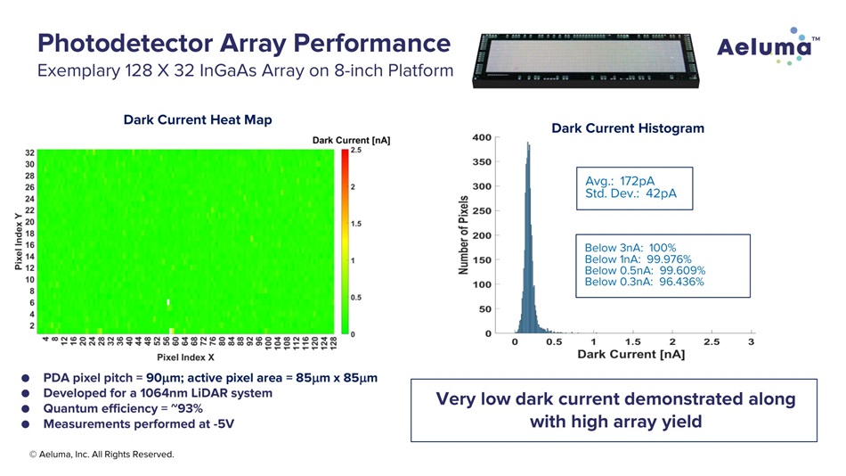
Ph o todetect o r A rr a y Perf o rma n ce Exemplary 128 X 32 InGaAs Array on 8 - inch Platform Dark C urrent H e at M ap ● P DA p i x el p i t ch = 9 0 m ; acti v e p i x el area = 8 5 m x 85 m ● Developed for a 1064nm LiDAR system ● Q ua n t u m eff i cie n cy = ~93% ● M eas u r eme n ts p erfor m ed at - 5V © Aelu m a , Inc. All R i g ht s R e serve d . Very low dark current demonstrated along with high array yie ld Below 3nA: 100% Below 1nA: 99.976% Below 0.5nA: 99.609% Below 0.3nA: 96.436% Dark C urrent H i st o g r a m Avg.: 172pA Std. Dev.: 4 2p A
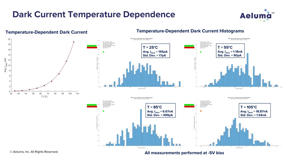
Dark Cur r ent Temper a ture Dep e ndence Temperature - Dependent Dark Current © Aelu m a , Inc. All R i g ht s R e serve d . All mea s ureme nts p e rformed at - 5V bias Temperature - Dependent Dark Current Histograms T = 25 ƒ C A v g. I d ar k = 1 55 pA St d. De v . = 1 7 pA T = 5 5 ƒ C Av g . I d ar k = 1 .1 8 n A Std. De v . = 9 0 pA T = 85 ƒ C Av g . I d ar k = 6 .67 n A Std. De v . = 49 9pA T = 1 0 5 ƒ C Av g . I d ar k = 1 8 .87 n A Std. De v . = 1 .54n A
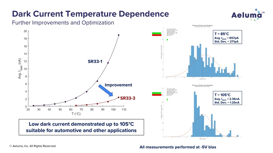
Dark Cur r ent Temper a ture Dep e ndence Further Improvements and Opti m ization T = 85 ƒ C Av g . I d ar k = 65 7 pA Std. De v . = 27 1 pA T = 1 0 5 ƒ C Av g . I d ar k = 2 . 3 6 n A Std. De v . = 1 . 2 5 n A SR3 3 - 1 S R 33 - 3 © Aelu m a , Inc. All R i g ht s R e serve d . All mea s ureme nts p e rformed at - 5V bias Improvement Low d a rk c urren t d e m ons t r a t ed up t o 10 5 ƒ C suitable for automotive and other applications
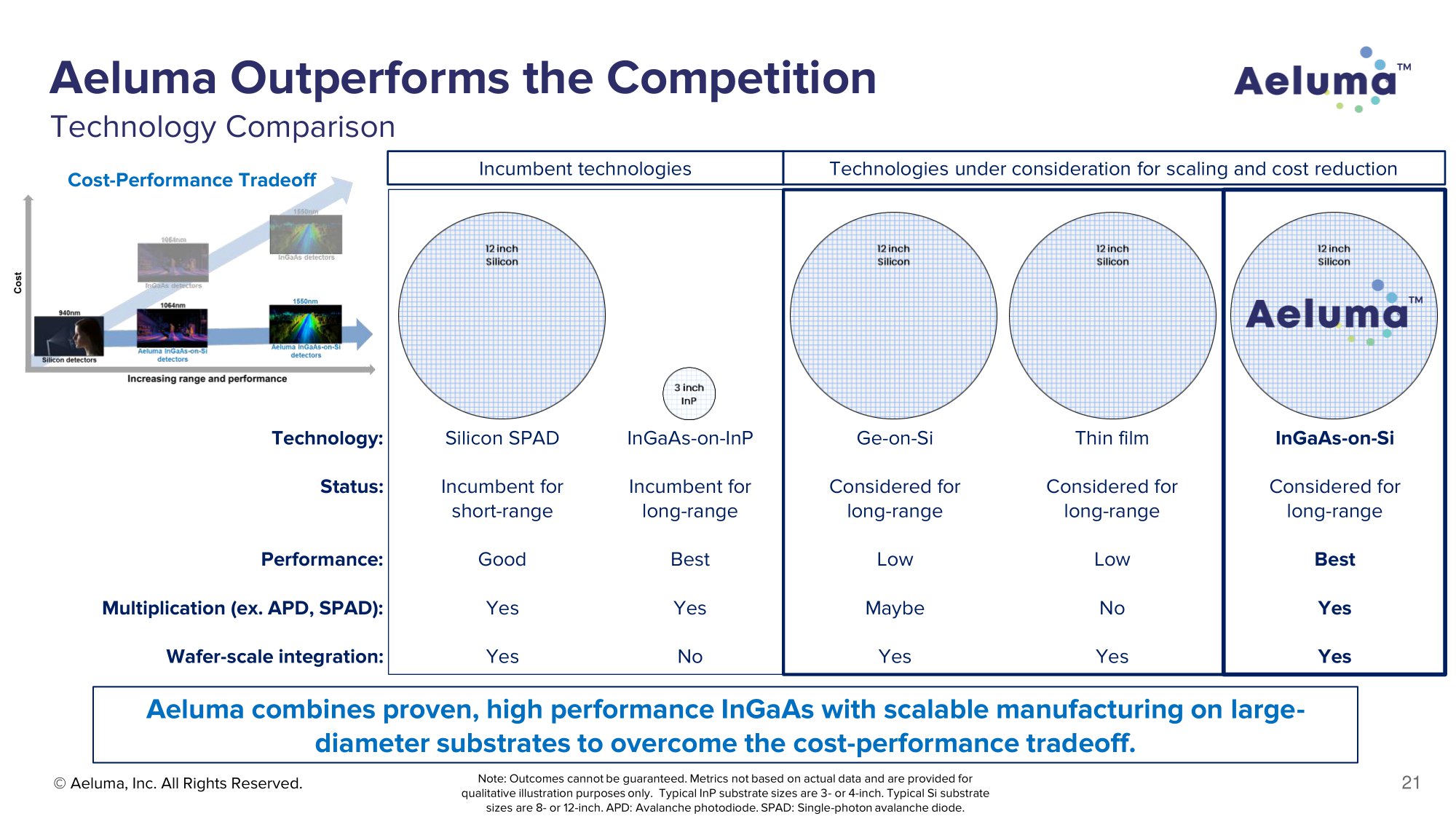
© Aelu m a , Inc. All R i g ht s R e serve d . Note: Outcomes cannot be guaranteed. Metrics not based on actual data and are provided for qualitative illustration purposes only. Typical InP substrate sizes are 3 - or 4 - inch. Typical Si substrate sizes are 8 - or 12 - inch. APD: Avalanche photodiode. SPAD: Single - photon avalanche diode. Ae luma Out p e rfor m s the Co m p e t i t i on Technology Comparison Technologies under consideration for scaling and cost reduction Incumbent t echn o l o gies InGaAs - on - Si T h i n f ilm Ge - on - Si InGaAs - on - InP Silic o n SPAD C o nside r ed fo r long - range C o nside r ed fo r long - range C o nside r ed fo r long - range Incumbent fo r long - range Incumbent fo r short - range Best Low Low Best Good Yes No Maybe Yes Yes Yes Yes Yes No Yes Aeluma combines proven, high performance InGaAs with scalable manufacturing on large - diameter substrates to overcome the cost - performance tradeoff. Technology: Status: Pe rform an c e: Multi p li c ation ( ex . AP D , SP A D ) : W a fer - s cale integ ratio n: 21 Co s t - Pe rform an c e T rad e o ff
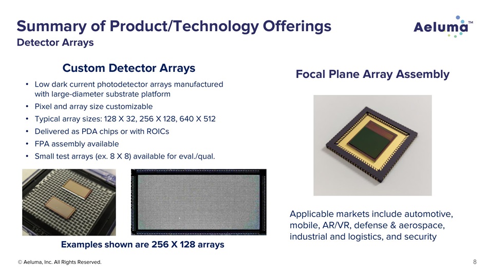
Summary of Product/Technology Offerings D e te ct o r Arrays Cu s tom De t ect or Arrays • Low dark current photodetector arrays manufactured w i t h l ar g e - d i amet e r s ub s t ra t e pla t f o rm • Pixel and array size customizable • Typical array sizes: 128 X 32, 256 X 128, 640 X 512 • Delivered as PDA chips or with ROICs • FPA assembly available • Sm a l l t e s t a rrays (ex. 8 X 8) ava i l a b l e f o r e va l ./qual . Exam p l es shown a re 256 X 128 a rrays Focal Plane Array As se mbly Appl i ca b l e m a r ke t s i n cl u de a u t o m ot i ve, m ob i le, AR/VR, defe n s e & ae r ospac e , industrial and logistics, and security © Aelu m a , Inc. All R i g ht s R e serve d . 8
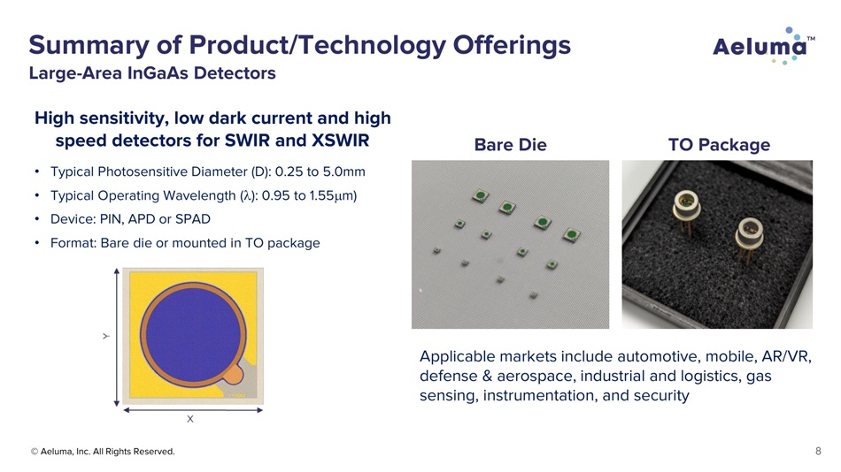
Summary of Product/Technology Offerings Large - Area InGaAs Detectors High sensitivity, low dark current and high s p ee d de te ct o rs f or SWIR and XSWIR • Typical Photosensitive Diameter (D): 0.25 to 5.0mm • Typi c al O p e ra t i ng Wavel e n g t h ( ): 0. 9 5 t o 1.55 m) • D e vi c e : P IN, AP D or S P AD • Forma t : Ba re d i e or mount e d i n TO pa c k age Bare D ie T O Pa c kage © Aelu m a , Inc. All R i g ht s R e serve d . 8 Applicable markets include automotive, mobile, AR/VR, defe n s e & ae r ospace, i n d u s t r ial and log i s t ic s , gas sensing, instrumentation, and security
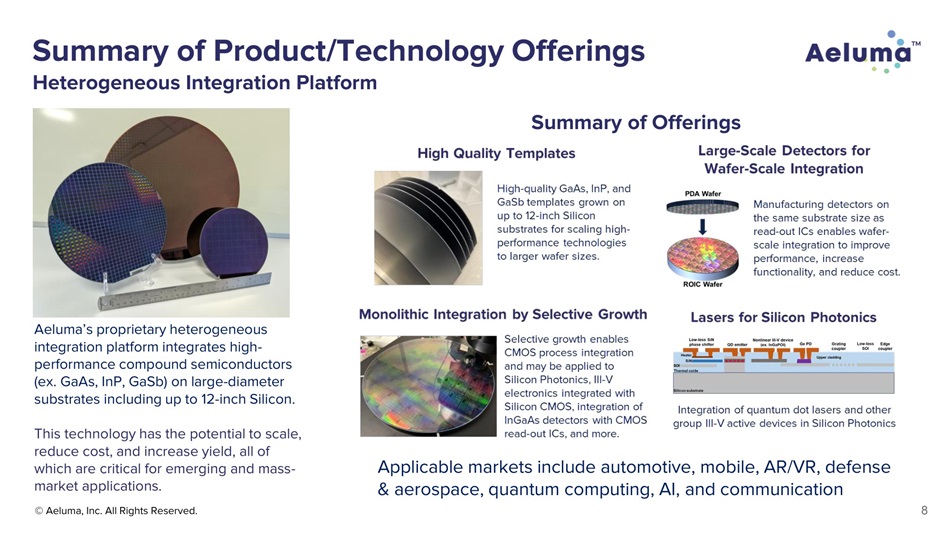
Summary of Product/Technology Offerings Applicable markets include automotive, mobile, AR/VR, defense & ae r o s pace, q u an t u m compu t i n g, AI, and com m un i cat i on Heterogeneous Integration Platform Summ ary of Of f e ri ngs © Aelu m a , Inc. All R i g ht s R e serve d . 8 Aeluma’s proprietary heterogeneous i n teg r a ti o n p l a tfo r m i n teg r ates h i g h - p erfor m a n c e c o m p o un d se m i c o n d uc t o r s (ex . G a A s, InP, G a Sb) on l a r g e - di a meter s ubs t r ates i n c l u di n g u p to 1 2 - i n c h Si l i c o n . T h i s tec h n o l ogy has the p o ten tial to s c a l e, reduce cost, and increase yield, all of w h i c h a r e c ri ti c a l fo r emer gin g a n d m a s s - market applications.
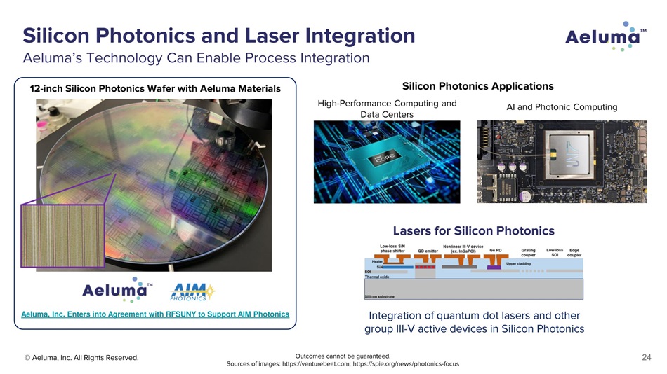
© Aelu m a , Inc. All R i g ht s R e serve d . Silicon Photonics and Laser Integration Aeluma’s Technology Can Enable Process Integration 12 - inch Silicon Photonics Wafer with Aeluma Materials Outcomes cannot be guaranteed. 24 Data Cen t e r s AI and Photonic Computing Silicon Photonics Applications High - Performance Computing and Aeluma, Inc. Enters into Agreement with RFSUNY to Support AIM Photonics Las ers f o r Sil i c on Phot onic s Integration of quantum dot lasers and other group III - V active devices in Silicon Photonics Sources of images: https://venturebeat.com; https://spie.org/news/photonics - focus
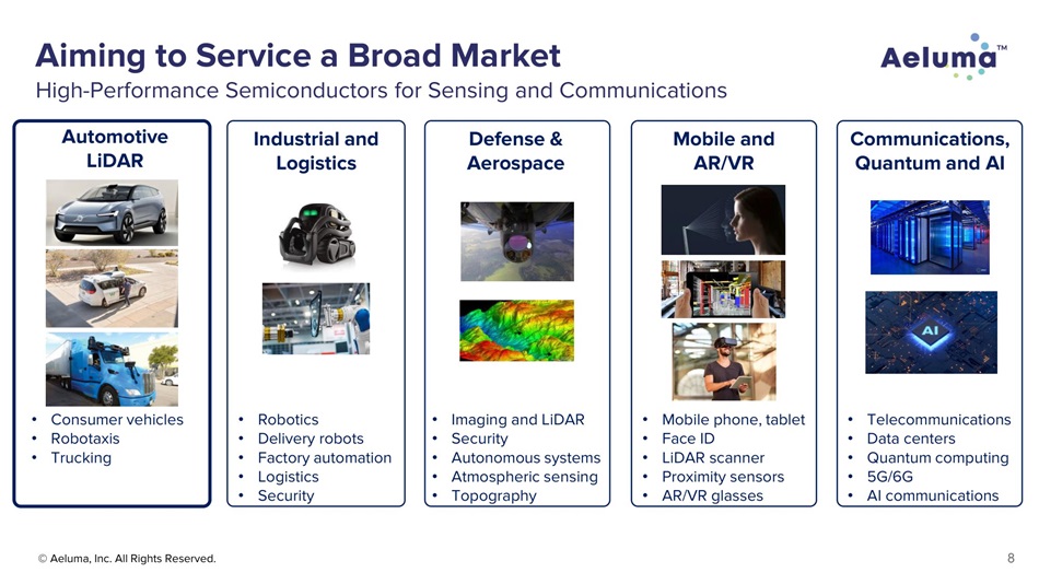
Au t omot i v e LiDAR Aiming to Service a Broad Market High - Performance Semiconductors for Sensing and Communications • C on su m er vehi c le s • Robotaxis • Trucking In d us t ri a l a nd Logistics Defe n se & Aerospa c e Mob i l e a nd AR/VR C omm un i c a t i o n s, Q u a n t um a nd AI • Robotics • D el i very ro bo ts • F a c to r y a u to m a ti o n • Logistics • Security • Imaging and LiDAR • Security • A u t o n o m ou s s ys te ms • A tmo s p h e ri c s e n s i n g • Topography • M obi le ph on e, t a ble t • F a c e ID • LiDAR scanner • Pr o x i m i ty se n s o r s • AR/VR glasses • Telecommunications • D a ta c e n ters • Q u a n tum c o m p u ti n g • 5G/6G • AI communications © Aelu m a , Inc. All R i g ht s R e serve d . 8
Co n clus i o n s ● Large - diameter wafer platform capable of scaling InGaAs detector arrays and other te c h nologi e s f or c o n s umer m a rke ts includ i ng aut o m o tive and m o bi le ● Demonstrated very low dark current detector arrays on 8 - inch wafer platform with excellent pixel yield, wafer uniformity, and high - temperature performance ● Developed selective growth processes for monolithic integration on Silicon CMOS ● Technologies available include detector arrays, large - area detectors, and hete r o ge n o us inte gration pl at f o rm © Aelu m a , Inc. All R i g ht s R e serve d . Visit Ae luma at Boot h 5143 info@aeluma.com | www.aeluma.com