Exhibit 99.1
Investor Presentatio n December 12, 2022 © Aeluma, Inc. All Rights Reserved. Sensing Reimagined TM
Forward Looking Statements Aeluma, Inc. All Rights Reserved. This presentation contains summary information about Aeluma, Inc . (“Aeluma”) as of the date hereof . The information in this presentation is of general background and contains an overview and summary of certain data selected by the management of Aeluma . It does not purport to be complete . This presentation is not a prospectus, disclosure document or offering document under the law of any jurisdiction . It is for informational purposes only . This presentation is not investment or financial product advice (nor tax, accounting or legal advice) and is not intended to be used for the basis of making an investment decision . A recipient must make their own independent investigations, consideration and evaluation of Aeluma and the offer and Aeluma recommends that investors should obtain their own professional advice before making any investment decisions in the company . This investor presentation shall also not constitute an offer to sell or the solicitation of an offer to buy any securities, nor shall there be any sale of securities in any states or jurisdictions in which such offer, solicitation or sale would be unlawful prior to registration or qualification under the securities laws of any such jurisdiction . No registered offering of securities shall be made except by means of a prospectus meeting the requirements of section 10 of the Securities Act of 1933 , as amended . This document has been prepared based on information available at the time of presentation . No representation or warranty, express or implied, is made as to the fairness, accuracy or completeness of the information, opinions and conclusions contained in this presentation or any omission from this presentation or of any other written or oral information or opinions provided now or in the future to any person . While reasonable care has been taken to ensure that facts stated in this presentation are accurate and/or that the opinions expressed are fair and reasonable, no reliance can be placed for any purpose whatsoever on the information contained in this document or its completeness . To the maximum extent permitted by law, neither Aeluma nor their respective officers, directors, employees, advisors and agents, nor any other person, accepts any liability as to or in relation to the accuracy or completeness of the information, statements, opinions or matters (express or implied) arising out of, contained in or derived from this presentation or any omission from this presentation or of any other written or oral information or opinions provided now or in the future to any person . Some of the statements appearing in this presentation are in the nature of forward looking statements . You should be aware that such statements are predictions based on assumptions, and are subject to inherent risks and uncertainties . Those risks and uncertainties include factors and risks specific to the industry in which Aeluma operates as well as general economic conditions, prevailing exchange rates and interest rates and conditions in the financial markets and other factors that are in some cases beyond Aeluma's control . As a result, any or all of the Aeluma’s forward - looking statements in this presentation may turn out to be inaccurate and actual results may be materially different than those expressed in such forward - looking statements . Except as required by law, we are under no duty to update or revise any of the forward - looking statements, whether as a result of new information, future events or otherwise, after the date of this presentation . These forward - looking statements speak only as of the date of this presentation, and we assume no obligation to update or revise these forward - looking statements for any reason . 2
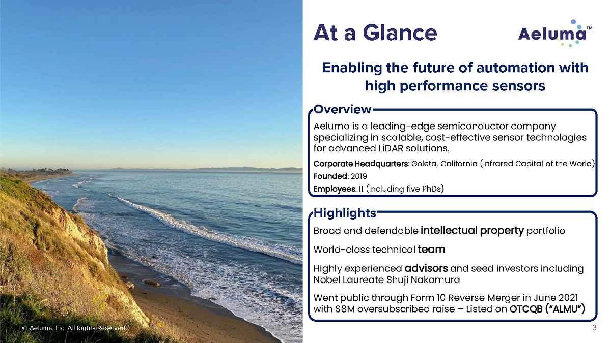
At a Glance © Aeluma, Inc. All Rights Reserved. Enabling the future of automation with high performance sensors Overvie w Aeluma is a leading - edge semiconductor company specializing in scalable, cost - effective sensor technologies for advanced LiDAR solutions. Corporate Headquarters : Goleta, California (Infrared Capital of the World) Founded : 2019 Employees : 11 (including five PhDs) Highlights Broad and defendable intellectual property portfolio World - class technical team Highly experienced advisors and seed investors including Nobel Laureate Shuji Nakamura Went public through Form 10 Reverse Merger in June 2021 with $8M oversubscribed raise – Listed on OTCQB (“ALMU”) 3
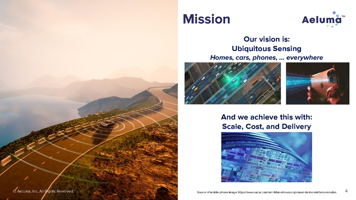
Our vision is: Ubiquitous Sensing Homes, cars, phones, … everywhere And we achieve this with: Scale, Cost, and Delivery Missio n © Aeluma, Inc. All Rights Reserved. Source of mobile phone image: https:// www.sacyr.com/en/ - /lidar - el - nuevo - ojo - laser - de - los - telefonos - moviles 4
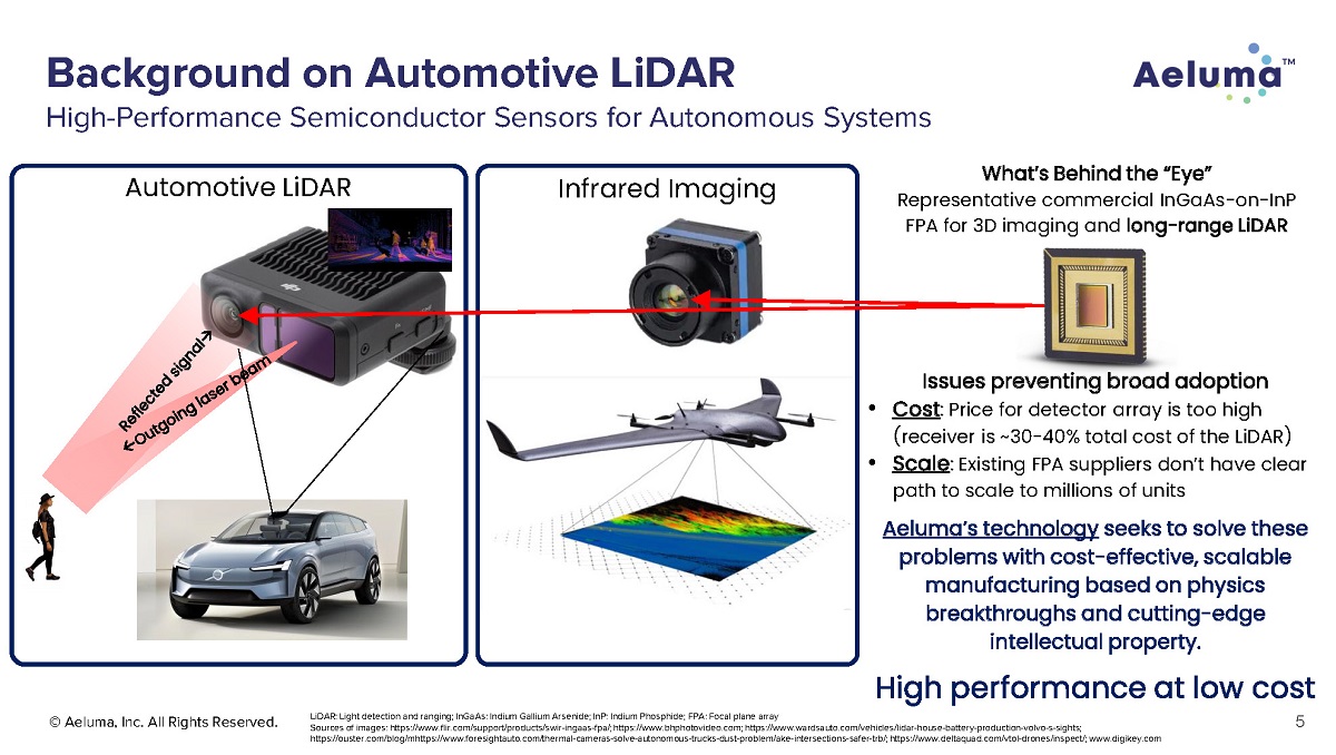
Background on Automotive LiDAR High - Performance Semiconductor Sensors for Autonomous Systems © Aeluma, Inc. All Rights Reserved. 5 LiDAR: Light detection and ranging; InGaAs: Indium Gallium Arsenide; InP: Indium Phosphide; FPA: Focal plane array Sources of images: https://www.flir.com/support/products/swir - ingaas - fpa/; https://www.bhphotovideo.com; https:// www.wardsauto.com/vehicles/lidar - house - battery - production - volvo - s - sights; https://ouster.com/blog/mhttps://www.foresightauto.com/thermal - cameras - solve - autonomous - trucks - dust - problem/ake - intersections - sa fer - trb/; https:// www.deltaquad.com/vtol - drones/inspect/; www.digikey.com What’s Behind the “Eye” Representative commercial InGaAs - on - InP FPA for 3D imaging and long - range LiDAR Issues preventing broad adoption • Cost : Price for detector array is too high (receiver is ~30 - 40% total cost of the LiDAR) • Scale : Existing FPA suppliers don’t have clear path to scale to millions of units Aeluma’s technology seeks to solve these problems with cost - effective, scalable manufacturing based on physics breakthroughs and cutting - edge intellectual property. High performance at low cost Automotive LiDAR Infrared Imaging
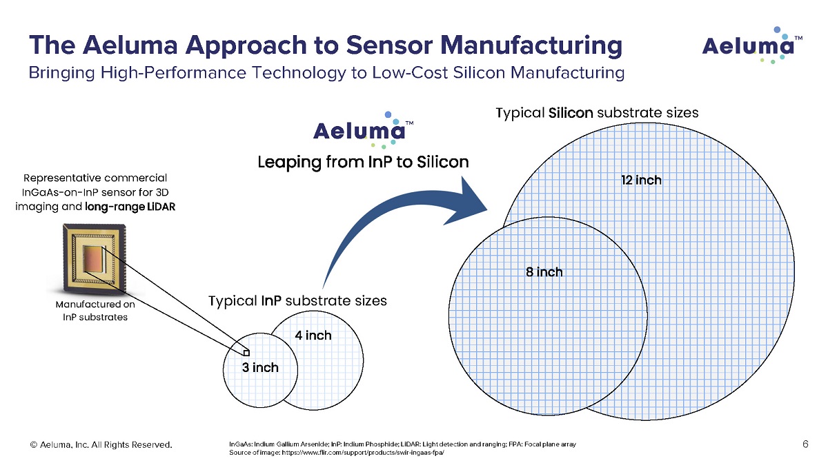
The Aeluma Approach to Sensor Manufacturing Bringing High - Performance Technology to Low - Cost Silicon Manufacturing © Aeluma, Inc. All Rights Reserved. 6 InGaAs: Indium Gallium Arsenide; InP: Indium Phosphide; LiDAR: Light detection and ranging; FPA: Focal plane array Source of image: https:// www.flir.com/support/products/swir - ingaas - fpa/ Typical InP substrate sizes Typical Silicon substrate sizes Leaping from InP to Silicon Representative commercial InGaAs - on - InP sensor for 3D imaging and long - range LiDAR Manufactured on InP substrates 4 inch 3 inch 8 inch 12 inch
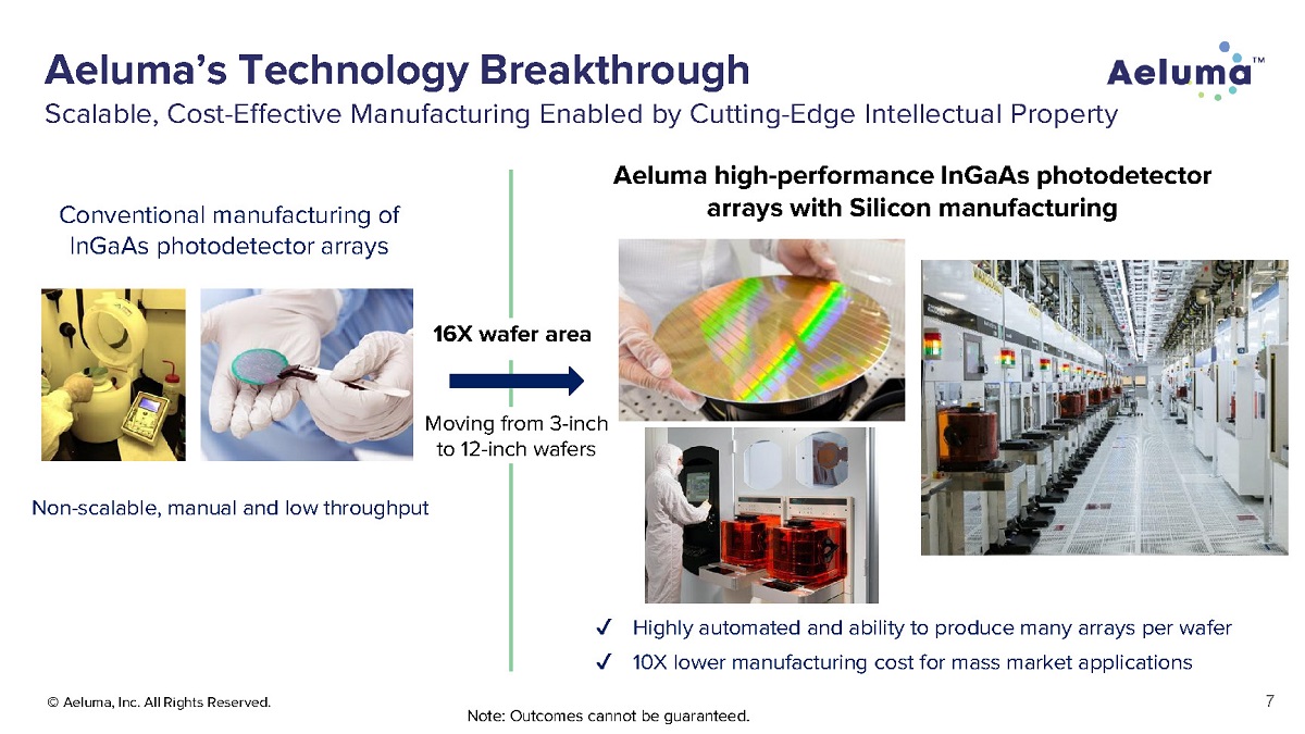
Conventional manufacturing of InGaAs photodetector arrays Aeluma high - performance InGaAs photodetector arrays with Silicon manufacturing ط Highly automated and ability to produce many arrays per wafer ط 10X lower manufacturing cost for mass market applications 16X wafer area Moving from 3 - inch to 12 - inch wafers Non - scalable, manual and low throughput Note: Outcomes cannot be guaranteed. © Aeluma, Inc. All Rights Reserved. Aeluma’s Technology Breakthrough Scalable, Cost - Effective Manufacturing Enabled by Cutting - Edge Intellectual Property 7
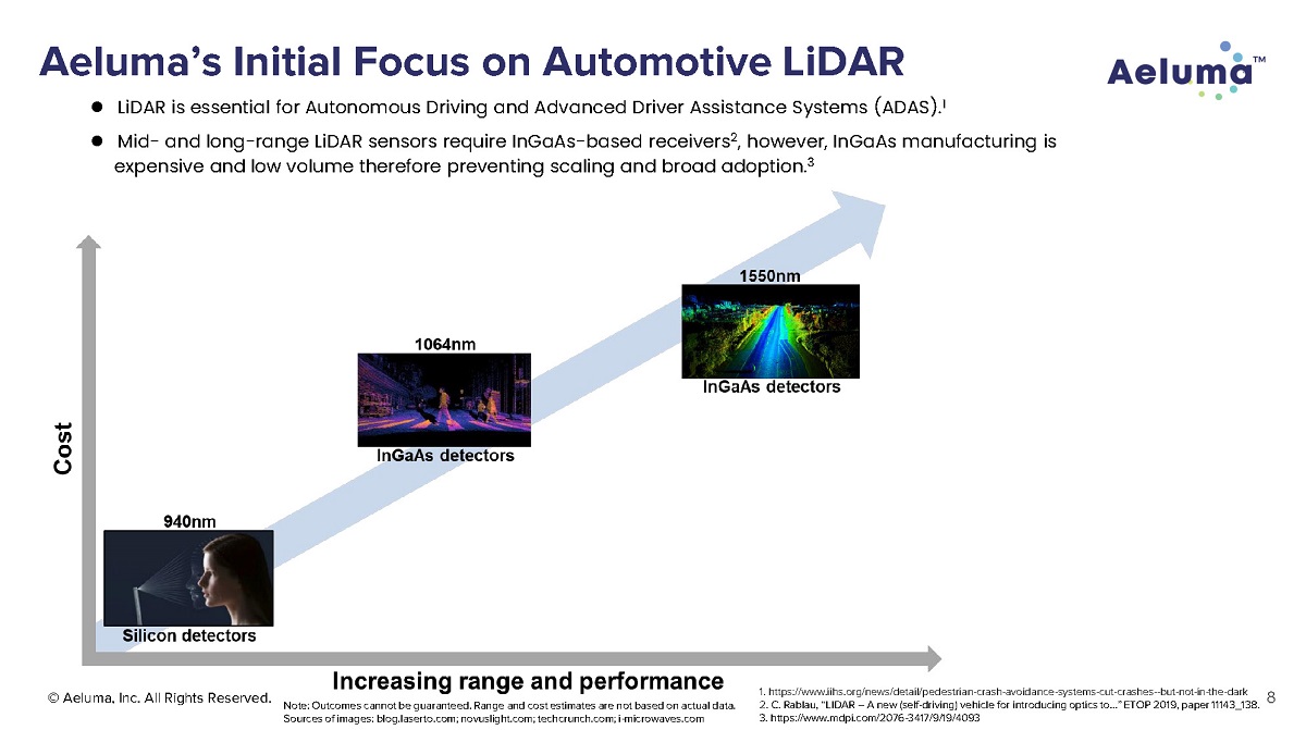
© Aeluma, Inc. All Rights Reserved. Aeluma’s Initial Focus on Automotive LiDAR ● LiDAR is essential for Autonomous Driving and Advanced Driver Assistance Systems (ADAS). 1 ● Mid - and long - range LiDAR sensors require InGaAs - based receivers 2 , however, InGaAs manufacturing is expensive and low volume therefore preventing scaling and broad adoption. 3 1. https:// www.iihs.org/news/detail/pedestrian - crash - avoidance - systems - cut - crashes - - but - not - in - the - dark Note: Outcomes cannot be guaranteed. Range and cost estimates are not based on actual data. 2. C. Rablau, “LIDAR – A new (self - driving) vehicle for introducing optics to...” ETOP 2019, paper 11143_138. Sources of images: blog.laserto.com; novuslight.com; techcrunch.com; i - microwaves.com 3. https:// www.mdpi.com/2076 - 3417/9/19/4093 8
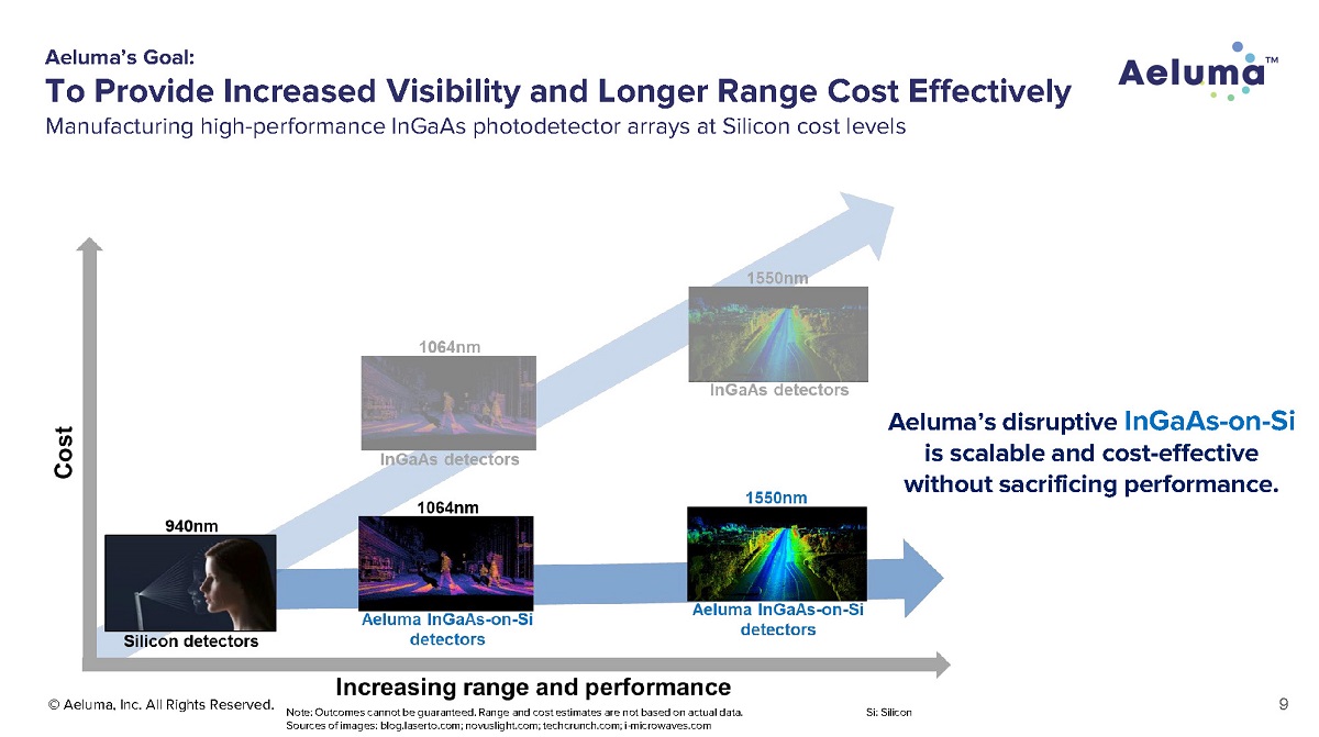
Si: Silicon Aeluma’s Goal: To Provide Increased Visibility and Longer Range Cost Effectively Manufacturing high - performance InGaAs photodetector arrays at Silicon cost levels Aeluma’s disruptive InGaAs - on - Si is scalable and cost - effective without sacrificing performance. © Aeluma, Inc. All Rights Reserved. Note: Outcomes cannot be guaranteed. Range and cost estimates are not based on actual data. Sources of images: blog.laserto.com; novuslight.com; techcrunch.com; i - microwaves.com 9
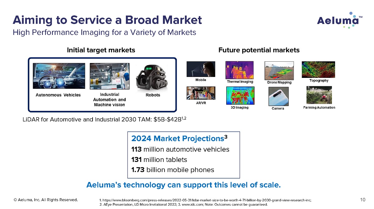
© Aeluma, Inc. All Rights Reserved. Aeluma’s technology can support this level of scale. 1. https:// www.bloomberg.com/press - releases/2022 - 05 - 31/lidar - market - size - to - be - worth - 4 - 71 - billion - by - 2030 - grand - view - research - inc; 2. AEye Presentation, LD Micro Invitational 2022; 3. www.idc.com; Note: Outcomes cannot be guaranteed. Initial target markets Future potential markets LiDAR for Automotive and Industrial 2030 TAM: $5B - $42B 1,2 2024 Market Projections 3 113 million automotive vehicles 131 million tablets 1.73 billion mobile phones Aiming to Service a Broad Market High Performance Imaging for a Variety of Markets 10
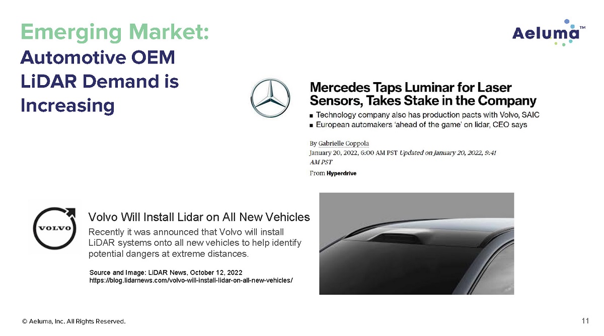
© Aeluma, Inc. All Rights Reserved. 11 Emerging Market: Automotive OEM LiDAR Demand is Increasing Volvo Will Install Lidar on All New Vehicles Recently it was announced that Volvo will install LiDAR systems onto all new vehicles to help identify potential dangers at extreme distances. Source and Image: LiDAR News, October 12, 2022 https://blog.lidarnews.com/volvo - will - install - lidar - on - all - new - vehicles/
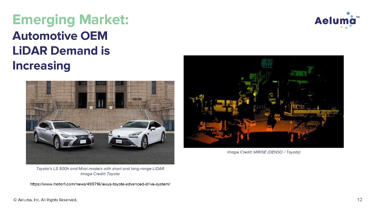
Emerging Market: Automotive OEM LiDAR Demand is Increasing © Aeluma, Inc. All Rights Reserved. 12 Image Credit: MIRISE (DENSO / Toyota) Toyota’s LS 500h and Mirai models with short and long - range LiDAR Image Credit: Toyota https:// www.motor1.com/news/499716/lexus - toyota - advanced - drive - system/
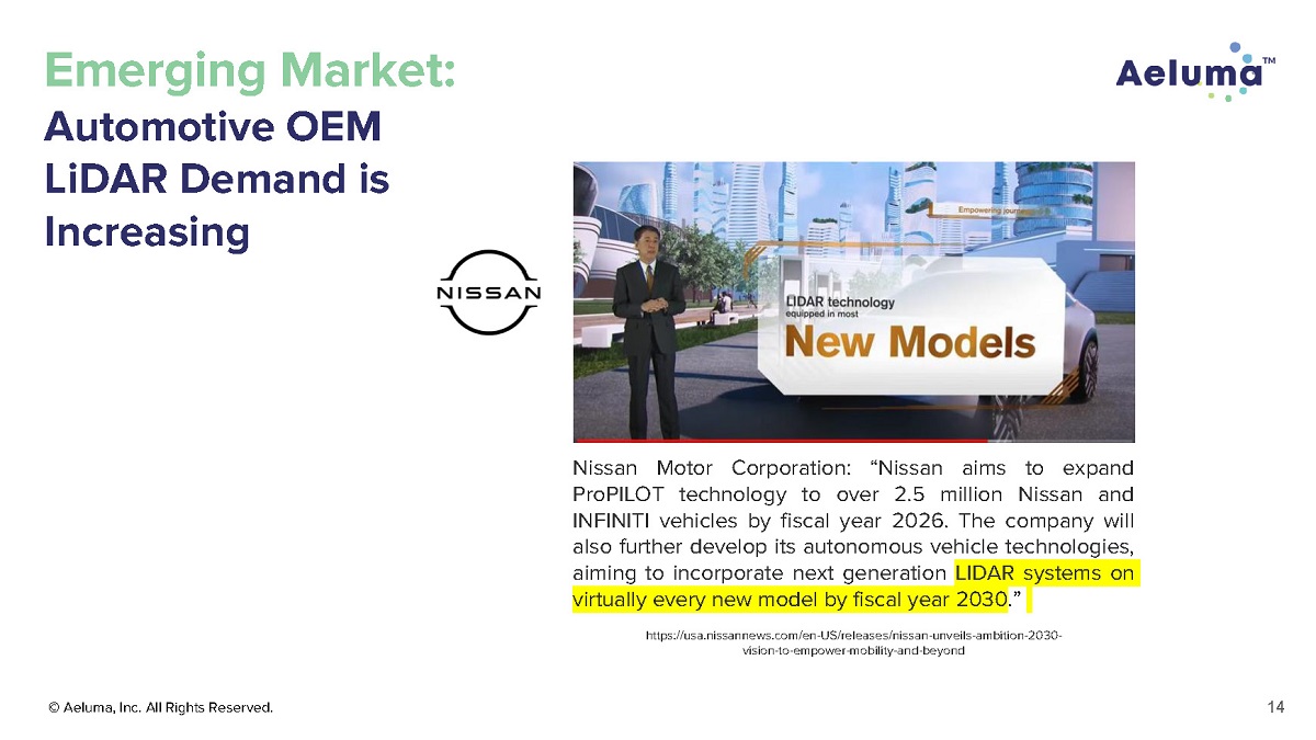
© Aeluma, Inc. All Rights Reserved. Nissan Motor Corporation : “Nissan aims to expand ProPILOT technology to over 2 . 5 million Nissan and INFINITI vehicles by fiscal year 2026 . The company will also further develop its autonomous vehicle technologies, aiming to incorporate next generation LIDAR systems on virtually every new model by fiscal year 2030 .” https://usa.nissannews.com/en - US/releases/nissan - unveils - ambition - 2030 - vision - to - empower - mobility - and - beyond 14 Emerging Market: Automotive OEM LiDAR Demand is Increasing
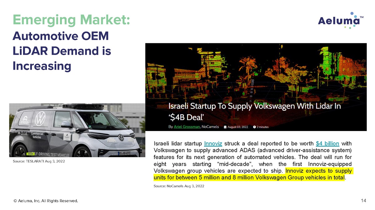
Emerging Market: Automotive OEM LiDAR Demand is Increasing © Aeluma, Inc. All Rights Reserved. Israeli lidar startup Innoviz struck a deal reported to be worth $ 4 billion with Volkswagen to supply advanced ADAS (advanced driver - assistance system) features for its next generation of automated vehicles . The deal will run for eight years starting “mid - decade”, when the first Innoviz - equipped Volkswagen group vehicles are expected to ship. Innoviz expects to supply units for between 5 million and 8 million Volkswagen Group vehicles in total . Source: TESLARATI Aug 3, 2022 Source: NoCamels Aug 3, 2022 14
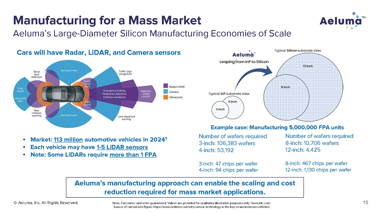
Manufacturing for a Mass Market © Aeluma, Inc. All Rights Reserved. 15 Aeluma’s Large - Diameter Silicon Manufacturing Economies of Scale Cars will have Radar, LiDAR, and Camera sensors Note: Outcomes cannot be guaranteed. Values are provided for qualitative illustration purposes only. 1 www.idc.com. Source of car/sensors figure: https:// www.eetimes.com/why - sensor - technology - is - the - key - to - autonomous - vehicles/ • Market: 113 million automotive vehicles in 2024 1 • Each vehicle may have 1 - 5 LiDAR sensors • Note: Some LiDARs require more than 1 FPA Number of wafers required 3 inch: 106,383 wafers 4 inch: 53,192 3 inch: 47 chips per wafer 4 inch: 94 chips per wafer Example case: Manufacturing 5,000,000 FPA units Number of wafers required 8 - inch: 10,706 wafers 12 - inch: 4,425 8 - inch: 467 chips per wafer 12 - inch: 1,130 chips per wafer Aeluma’s manufacturing approach can enable the scaling and cost reduction required for mass market applications.
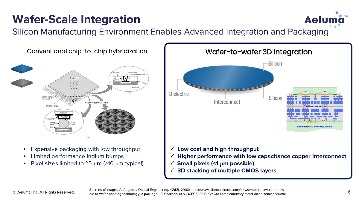
Wafer - Scale Integration Silicon Manufacturing Environment Enables Advanced Integration and Packaging © Aeluma, Inc. All Rights Reserved. 16 Sources of images: A. Rogalski, Optical Engineering, 42(12), 2003; https:// www.allaboutcircuits.com/news/moores - law - xperi - new - die - to - wafer - bonding - technology - ic - package/; E. Charbon, et al., ICECS, 2018; CMOS: complementary metal - oxide semiconductor Conventional chip - to - chip hybridization Wafer - to - wafer 3D Integration • Expensive packaging with low throughput • Limited performance indium bumps • Pixel sizes limited to ~5 m (>10 m typical) x Low cost and high throughput x Higher performance with low capacitance copper interconnect x Small pixels (<1 m possible) x 3D stacking of multiple CMOS layers
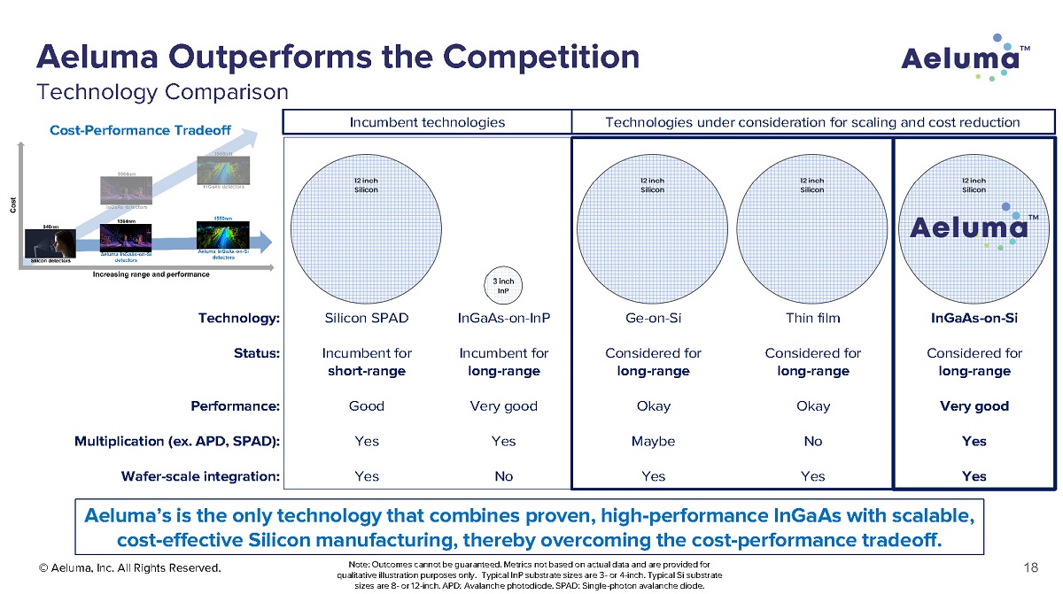
© Aeluma, Inc. All Rights Reserved. Note: Outcomes cannot be guaranteed. Metrics not based on actual data and are provided for qualitative illustration purposes only. Typical InP substrate sizes are 3 - or 4 - inch. Typical Si substrate sizes are 8 - or 12 - inch. APD: Avalanche photodiode. SPAD: Single - photon avalanche diode. Aeluma Outperforms the Competition Technology Comparison Aeluma’s is the only technology that combines proven, high - performance InGaAs with scalable, cost - effective Silicon manufacturing, thereby overcoming the cost - performance tradeoff. Technology: Status: Performanc e: Multiplication (ex. APD, SPAD): Wafer - scale integration: Incumbent technologies Technologies under consideration for scaling and cost reduction Silicon SPAD InGaAs - on - InP Ge - on - Si Thin film InGaAs - on - Si Incumbent for short - range Incumbent for long - range Considered for long - range Considered for long - range Considered for long - range Good Very good Okay Okay Very good Yes Yes Maybe No Yes Yes No Yes Yes Yes 18 Cost - Performance Tradeoff
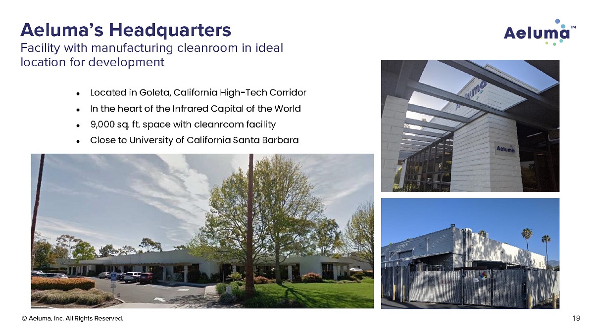
● Located in Goleta, California High - Tech Corridor ● In the heart of the Infrared Capital of the World ● 9,000 sq. ft. space with cleanroom facility ● Close to University of California Santa Barbara © Aeluma, Inc. All Rights Reserved. Aeluma’s Headquarters Facility with manufacturing cleanroom in ideal location for development 19
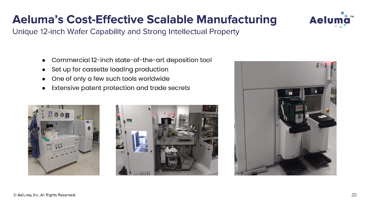
© Aeluma, Inc. All Rights Reserved. Aeluma’s Cost - Effective Scalable Manufacturing Unique 12 - inch Wafer Capability and Strong Intellectual Property ● Commercial 12 - inch state - of - the - art deposition tool ● Set up for cassette loading production ● One of only a few such tools worldwide ● Extensive patent protection and trade secrets 20
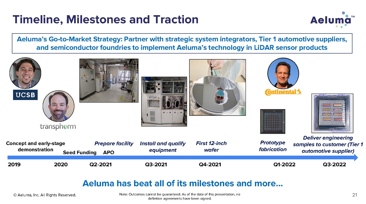
© Aeluma, Inc. All Rights Reserved. Aeluma’s Go - to - Market Strategy: Partner with strategic system integrators, Tier 1 automotive suppliers, and semiconductor foundries to implement Aeluma’s technology in LiDAR sensor products Aeluma has beat all of its milestones and more… Note: Outcomes cannot be guaranteed. As of the date of this presentation, no Timeline, Milestones and Traction Prepare facility Install and qualify equipment First 12 - inch wafer Prototype fabrication Concept and early - stage demonstratio n 201 9 Q3 - 2022 Seed Funding APO 2020 Q2 - 2021 Q3 - 2021 Q4 - 2021 Q1 - 2022 Deliver engineering samples to customer (Tier 1 automotive supplier) 21
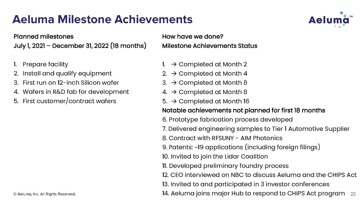
© Aeluma, Inc. All Rights Reserved. Aeluma Milestone Achievements Planned milestones July 1, 2021 – December 31, 2022 (18 months) 1. Prepare facility 2. Install and qualify equipment 3. First run on 12 - inch Silicon wafer 4. Wafers in R&D fab for development 5. First customer/contract wafers How have we done? Milestone Achievements Status 1. Completed at Month 2 2. Completed at Month 4 3. Completed at Month 8 4. Completed at Month 8 5. Completed at Month 16 Notable achievements not planned for first 18 months 6. Prototype fabrication process developed 7. Delivered engineering samples to Tier 1 Automotive Supplier 8. Contract with RFSUNY - AIM Photonics 9. Patents: ~19 applications (including foreign filings) 10. Invited to join the Lidar Coalition 11. Developed preliminary foundry process 12. CEO interviewed on NBC to discuss Aeluma and the CHIPS Act 13. Invited to and participated in 3 investor conferences 14. Aeluma joins major Hub to respond to CHIPS Act program 22
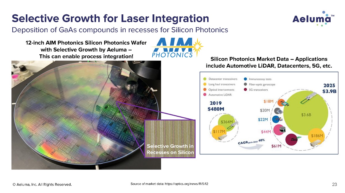
© Aeluma, Inc. All Rights Reserved. Selective Growth for Laser Integration Deposition of GaAs compounds in recesses for Silicon Photonics 12 - inch AIM Photonics Silicon Photonics Wafer with Selective Growth by Aeluma – This can enable process integration! Selective Growth in Recesses on Silicon Source of market data: https://optics.org/news/11/5/12 Silicon Photonics Market Data – Applications include Automotive LiDAR, Datacenters, 5G, etc. 23
© Aeluma, Inc. All Rights Reserved. Aeluma Intellectual Property Strategy Strategy and Status ● Trade Secrets ○ Secret information that provides a competitive advantage ○ Reasonable precautions taken to preserve secrecy ○ Examples: confidential business information, process recipes, chip designs, layer structures, employees and skill levels ● Patents (~19 applications including country filings) ○ Aim to cover nearly all aspects of technology including systems, applications, architectures, circuits, materials, packaging and assembly, process, device manufacturing, testing, structures ● Trademarks (“Aeluma TM ” and “Sensing reimagined TM ”) ● Agreements including Non - Disclosure Agreements Note: Outcomes cannot be guaranteed. 24
Our Leadership Team Vision, Entrepreneurship and Expertise Jonathan Klamkin, PhD Founder, CEO & Director Thomas Laux VP of Business Development Steven DenBaars, PhD Advisor, Seed Investor & Director Shuji Nakamura, PhD Seed Investor Jeffrey Shealy, PhD, MBA Advisor & Seed Investor Richard Ogawa, JD Advisor & Seed Investor © Aeluma, Inc. All Rights Reserved. John Paglia, PhD Director Palvi Mehta Director 25
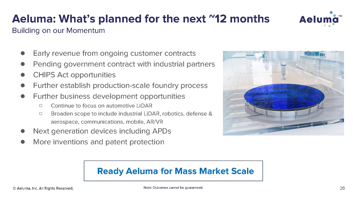
© Aeluma, Inc. All Rights Reserved. Aeluma: What’s planned for the next ~12 months Building on our Momentum ● Early revenue from ongoing customer contracts ● Pending government contract with industrial partners ● CHIPS Act opportunities ● Further establish production - scale foundry process ● Further business development opportunities ○ Continue to focus on automotive LiDAR ○ Broaden scope to include industrial LiDAR, robotics, defense & aerospace, communications, mobile, AR/VR ● Next generation devices including APDs ● More inventions and patent protection Ready Aeluma for Mass Market Scale Note: Outcomes cannot be guaranteed. 26
© Aeluma, Inc. All Rights Reserved. Company Contact: Jonathan Klamkin, CEO Aeluma, Inc. 805 - 351 - 2707 jonathan.klamkin@aeluma.com Sensing Reimagined TM